Vishay Isolated TrenchFET 2 Type P-Channel Power MOSFET, 1.1 A, 20 V Enhancement, 6-Pin SC-88 SI1967DH-T1-GE3
- N° de stock RS:
- 812-3108
- Référence fabricant:
- SI1967DH-T1-GE3
- Fabricant:
- Vishay

Offre groupée disponible
Consulter les options de prix de grosSous-total (1 ruban de 50 unités)*
20,05 €
(TVA exclue)
24,25 €
(TVA incluse)
Frais de livraison offerts pour toute commande de plus de 90,00 €
En stock
- Plus 150 unité(s) expédiée(s) à partir du 20 juillet 2026
Besoin de plus? Cliquez sur " Vérifier les dates de livraison " pour plus de détails
Unité | Prix par unité | le ruban* |
|---|---|---|
| 50 - 200 | 0,401 € | 20,05 € |
| 250 - 450 | 0,30 € | 15,00 € |
| 500 - 1200 | 0,281 € | 14,05 € |
| 1250 - 2450 | 0,241 € | 12,05 € |
| 2500 + | 0,209 € | 10,45 € |
*Prix donné à titre indicatif
- N° de stock RS:
- 812-3108
- Référence fabricant:
- SI1967DH-T1-GE3
- Fabricant:
- Vishay
Spécifications
Documentation technique
Législations et de normes
Détails du produit
Recherchez des produits similaires en sélectionnant un ou plusieurs attributs.
Sélectionner tout | Attribut | Valeur |
|---|---|---|
| Marque | Vishay | |
| Product Type | Power MOSFET | |
| Channel Type | Type P | |
| Maximum Continuous Drain Current Id | 1.1A | |
| Maximum Drain Source Voltage Vds | 20V | |
| Series | TrenchFET | |
| Package Type | SC-88 | |
| Mount Type | Surface | |
| Pin Count | 6 | |
| Maximum Drain Source Resistance Rds | 790mΩ | |
| Channel Mode | Enhancement | |
| Minimum Operating Temperature | -55°C | |
| Maximum Power Dissipation Pd | 1.25W | |
| Maximum Gate Source Voltage Vgs | 8V | |
| Typical Gate Charge Qg @ Vgs | 2.6nC | |
| Transistor Configuration | Isolated | |
| Maximum Operating Temperature | 150°C | |
| Length | 2.2mm | |
| Standards/Approvals | No | |
| Width | 1.35mm | |
| Height | 1mm | |
| Number of Elements per Chip | 2 | |
| Automotive Standard | No | |
| Sélectionner tout | ||
|---|---|---|
Marque Vishay | ||
Product Type Power MOSFET | ||
Channel Type Type P | ||
Maximum Continuous Drain Current Id 1.1A | ||
Maximum Drain Source Voltage Vds 20V | ||
Series TrenchFET | ||
Package Type SC-88 | ||
Mount Type Surface | ||
Pin Count 6 | ||
Maximum Drain Source Resistance Rds 790mΩ | ||
Channel Mode Enhancement | ||
Minimum Operating Temperature -55°C | ||
Maximum Power Dissipation Pd 1.25W | ||
Maximum Gate Source Voltage Vgs 8V | ||
Typical Gate Charge Qg @ Vgs 2.6nC | ||
Transistor Configuration Isolated | ||
Maximum Operating Temperature 150°C | ||
Length 2.2mm | ||
Standards/Approvals No | ||
Width 1.35mm | ||
Height 1mm | ||
Number of Elements per Chip 2 | ||
Automotive Standard No | ||
- Pays d'origine :
- CN
Vishay TrenchFET Series Power MOSFET, 20V Maximum Drain Source Voltage, 1.1A Maximum Continuous Drain Current - SI1967DH-T1-GE3
This power MOSFET is a P‑channel surface‑mount transistor designed for low‑voltage switching in Compact electronic systems. It operates as an enhancement‑mode device and is intended for board‑level power control where modest current handling and a small footprint are required.
Features and Benefits:
• 20V drain‑source rating enables low‑voltage system deployment • 1.1A continuous drain current supports light power switching • 790mΩ low Rds(on) reduces conduction losses during operation • 2.6nC typical gate charge permits Faster gate transitions • 1.25W power dissipation manages thermal load in small assemblies • Dual‑element isolated transistor allows paired switching arrangements
Applications
• Suitable for battery management and power rail switching in portable equipment • Ideal for load switching in industrial control modules • Used for reverse‑polarity protection in embedded systems • Can be used for signal level shifting in mixed‑voltage circuitry
What package should I plan for when designing the PCB?
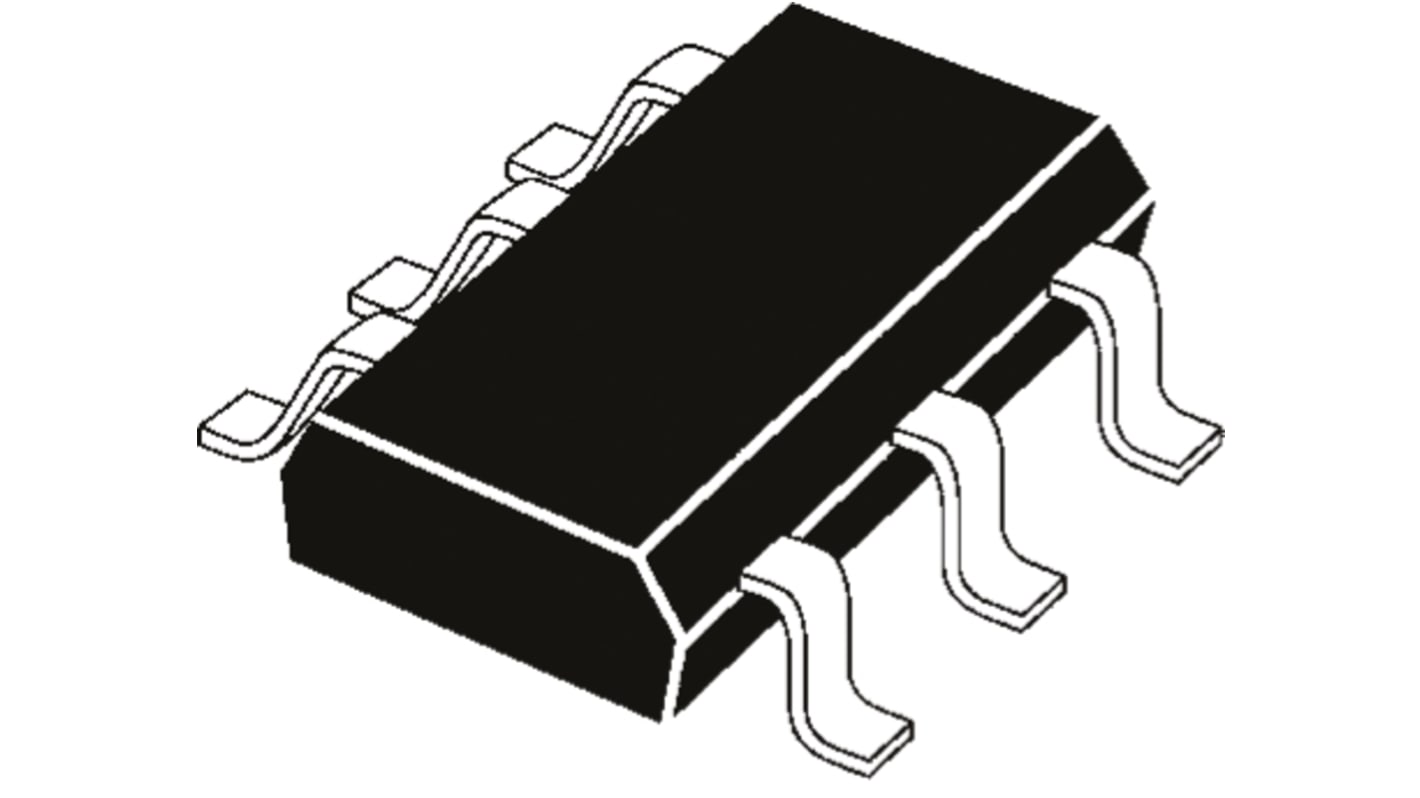
The device is supplied in a 6‑pin SC‑88 SMD package that occupies a Compact footprint suitable for high‑density boards.
How does temperature affect operation limits?
The component is specified for operation between -55°C and 150°C, defining the allowable ambient and junction environments for reliable switching.
Can this component be used in automotive systems?
It is not classified to automotive standards, so suitability should be evaluated against vehicular qualification requirements before use.
What gate voltage range is permissible for control signals?
Gate drive must not exceed an 8V gate‑to‑source limit to avoid device overstress.
How many transistor elements are on the chip and what configuration are they?
The chip contains two isolated elements configured to enable paired or independent switching arrangements.
Liens connexes
- Vishay Isolated TrenchFET 2 Type P-Channel Power MOSFET 20 V Enhancement, 6-Pin SC-88
- Vishay Isolated TrenchFET 2 Type P 700 mA 6-Pin SC-88 SI1553CDL-T1-GE3
- Vishay Isolated TrenchFET 2 Type N-Channel Power MOSFET 20 V Enhancement, 6-Pin SC-88 SI1922EDH-T1-GE3
- Vishay Isolated TrenchFET 2 Type P 700 mA 6-Pin SC-88
- Vishay Isolated TrenchFET 2 Type N-Channel Power MOSFET 20 V Enhancement, 6-Pin SC-88
- Vishay Isolated TrenchFET 2 Type P 300 mA 6-Pin SC-89-6 SI1029X-T1-GE3
- Vishay Isolated TrenchFET 2 Type P 135 mA 6-Pin SC-89-6 SI1025X-T1-GE3
- Vishay Isolated TrenchFET 2 Type P 4.5 A 6-Pin SC-70 SIA517DJ-T1-GE3