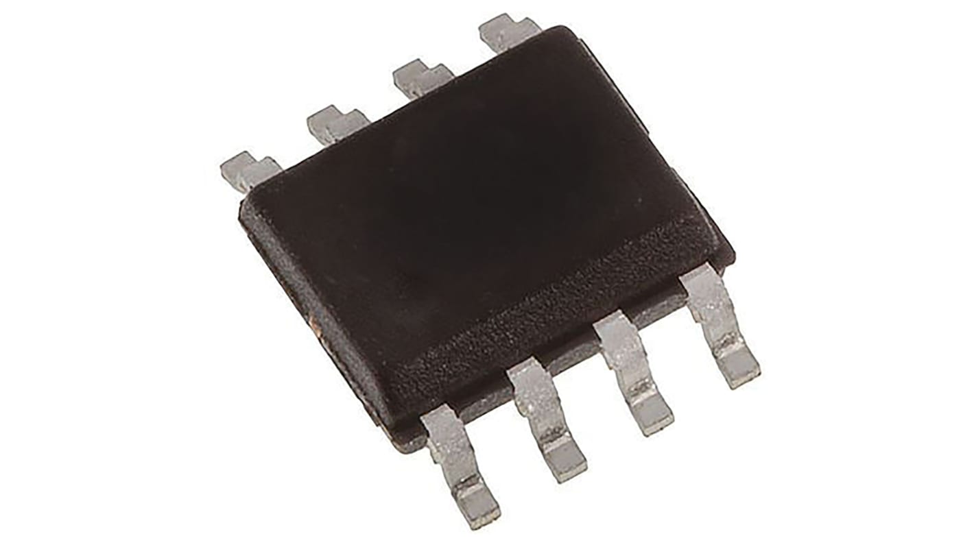
Vishay Si4178DY Type N-Channel MOSFET, 12 A, 30 V Enhancement, 8-Pin SOIC SI4178DY-T1-GE3
- N° de stock RS:
- 165-7249
- Référence fabricant:
- SI4178DY-T1-GE3
- Fabricant:
- Vishay

Sous-total (1 bobine de 2500 unités)*
565,00 €
(TVA exclue)
682,50 €
(TVA incluse)
Frais de livraison offerts pour toute commande de plus de 90,00 €
Temporairement en rupture de stock
- Expédition à partir du 26 novembre 2026
Besoin de plus? Cliquez sur " Vérifier les dates de livraison " pour plus de détails
Unité | Prix par unité | la bobine* |
|---|---|---|
| 2500 + | 0,226 € | 565,00 € |
*Prix donné à titre indicatif
- N° de stock RS:
- 165-7249
- Référence fabricant:
- SI4178DY-T1-GE3
- Fabricant:
- Vishay
Spécifications
Documentation technique
Législations et de normes
Détails du produit
Recherchez des produits similaires en sélectionnant un ou plusieurs attributs.
Sélectionner tout | Attribut | Valeur |
|---|---|---|
| Marque | Vishay | |
| Product Type | MOSFET | |
| Channel Type | Type N | |
| Maximum Continuous Drain Current Id | 12A | |
| Maximum Drain Source Voltage Vds | 30V | |
| Series | Si4178DY | |
| Package Type | SOIC | |
| Mount Type | Surface | |
| Pin Count | 8 | |
| Maximum Drain Source Resistance Rds | 33mΩ | |
| Channel Mode | Enhancement | |
| Maximum Gate Source Voltage Vgs | 25V | |
| Typical Gate Charge Qg @ Vgs | 7.5nC | |
| Minimum Operating Temperature | -55°C | |
| Maximum Power Dissipation Pd | 5W | |
| Forward Voltage Vf | 0.85V | |
| Maximum Operating Temperature | 150°C | |
| Length | 5mm | |
| Height | 1.55mm | |
| Standards/Approvals | RoHS | |
| Width | 4mm | |
| Automotive Standard | No | |
| Sélectionner tout | ||
|---|---|---|
Marque Vishay | ||
Product Type MOSFET | ||
Channel Type Type N | ||
Maximum Continuous Drain Current Id 12A | ||
Maximum Drain Source Voltage Vds 30V | ||
Series Si4178DY | ||
Package Type SOIC | ||
Mount Type Surface | ||
Pin Count 8 | ||
Maximum Drain Source Resistance Rds 33mΩ | ||
Channel Mode Enhancement | ||
Maximum Gate Source Voltage Vgs 25V | ||
Typical Gate Charge Qg @ Vgs 7.5nC | ||
Minimum Operating Temperature -55°C | ||
Maximum Power Dissipation Pd 5W | ||
Forward Voltage Vf 0.85V | ||
Maximum Operating Temperature 150°C | ||
Length 5mm | ||
Height 1.55mm | ||
Standards/Approvals RoHS | ||
Width 4mm | ||
Automotive Standard No | ||
- Pays d'origine :
- CN
Vishay Si4178DY Series MOSFET, 30V Maximum Drain Source Voltage, 12A Maximum Continuous Drain Current - SI4178DY-T1-GE3
This is a surface-mount N-channel MOSFET intended for power switching and high-current applications within electronic systems. It operates as an enhancement-mode transistor and is supplied in an SOIC-8 package for PCB mounting. The device supports moderate voltage switching and is suitable for designs requiring Compact power transistors with controlled gate-charge characteristics.
Features and Benefits:
• 30V maximum drain voltage enabling low-voltage power switching • 12A continuous drain current for handling high load currents • 33mΩ drain-source resistance for reduced conduction losses • 7.5nC typical gate charge for Faster switching transitions • 5W power dissipation capacity for sustained thermal performance • -55°C to 150°C operating range for wide thermal tolerance
Applications
• Suitable for DC power distribution switches in automation panels • Ideal for motor driver low-side switching in industrial drives • Used for load switching in power-management circuits for control systems • Can be used for synchronous rectification in Compact power converters • Suitable for battery protection and power-path control in machinery
What gate-voltage limits should be observed during design?
The gate-source voltage must not exceed ±25V to prevent gate-oxide stress and ensure reliable switching.
How should thermal management be approached on the PCB?
Given a 5W dissipation rating, provide adequate copper area and thermal vias to lower junction temperature during continuous high-current operation.
What pin-count and package considerations affect layout?
The device arrives in an 8-pin SOIC package, so track widths and pad spacing should accommodate surface-mount assembly and thermal conduction.
What electrical characteristic governs switching speed in Pulse applications?
The typical gate charge of 7.5nC is the key parameter influencing drive requirements and switching transition times when selecting gate drivers.
Liens connexes
- Vishay Si4178DY Type N-Channel MOSFET 30 V Enhancement, 8-Pin SOIC SI4178DY-T1-GE3
- Vishay Si4162DY Type N-Channel MOSFET 30 V Enhancement, 8-Pin SOIC
- Vishay TrenchFET Type N-Channel MOSFET 30 V Enhancement, 8-Pin SOIC
- Vishay Si4134DY Type N-Channel MOSFET 30 V Enhancement, 8-Pin SOIC
- Vishay Si4164DY Type N-Channel TrenchFET Power MOSFET 30 V Enhancement, 8-Pin SOIC
- Vishay Si4162DY Type N-Channel MOSFET 30 V Enhancement, 8-Pin SOIC SI4162DY-T1-GE3
- Vishay TrenchFET Type N-Channel MOSFET 30 V Enhancement, 8-Pin SOIC SI4128DY-T1-GE3
- Vishay Si4134DY Type N-Channel MOSFET 30 V Enhancement, 8-Pin SOIC Si4134DY-T1-GE3