Infineon C7 GOLD Type N-Channel MOSFET & Diode, 83 A, 650 V Enhancement, 10-Pin HDSOP
- N° de stock RS:
- 220-7417
- Référence fabricant:
- IPDD60R080G7XTMA1
- Fabricant:
- Infineon

Sous-total (1 bobine de 1700 unités)*
3 835,20 €
(TVA exclue)
4 641,00 €
(TVA incluse)
Frais de livraison offerts pour toute commande de plus de 90,00 €
En stock
- Plus 1 700 unité(s) expédiée(s) à partir du 20 juillet 2026
Besoin de plus? Cliquez sur " Vérifier les dates de livraison " pour plus de détails
Unité | Prix par unité | la bobine* |
|---|---|---|
| 1700 + | 2,256 € | 3 835,20 € |
*Prix donné à titre indicatif
- N° de stock RS:
- 220-7417
- Référence fabricant:
- IPDD60R080G7XTMA1
- Fabricant:
- Infineon
Spécifications
Documentation technique
Législations et de normes
Détails du produit
Recherchez des produits similaires en sélectionnant un ou plusieurs attributs.
Sélectionner tout | Attribut | Valeur |
|---|---|---|
| Marque | Infineon | |
| Channel Type | Type N | |
| Product Type | MOSFET & Diode | |
| Maximum Continuous Drain Current Id | 83A | |
| Maximum Drain Source Voltage Vds | 650V | |
| Package Type | HDSOP | |
| Series | C7 GOLD | |
| Mount Type | Surface | |
| Pin Count | 10 | |
| Maximum Drain Source Resistance Rds | 80mΩ | |
| Channel Mode | Enhancement | |
| Maximum Power Dissipation Pd | 174W | |
| Typical Gate Charge Qg @ Vgs | 42nC | |
| Forward Voltage Vf | 0.8V | |
| Height | 21.11mm | |
| Length | 6.6mm | |
| Standards/Approvals | No | |
| Automotive Standard | No | |
| Sélectionner tout | ||
|---|---|---|
Marque Infineon | ||
Channel Type Type N | ||
Product Type MOSFET & Diode | ||
Maximum Continuous Drain Current Id 83A | ||
Maximum Drain Source Voltage Vds 650V | ||
Package Type HDSOP | ||
Series C7 GOLD | ||
Mount Type Surface | ||
Pin Count 10 | ||
Maximum Drain Source Resistance Rds 80mΩ | ||
Channel Mode Enhancement | ||
Maximum Power Dissipation Pd 174W | ||
Typical Gate Charge Qg @ Vgs 42nC | ||
Forward Voltage Vf 0.8V | ||
Height 21.11mm | ||
Length 6.6mm | ||
Standards/Approvals No | ||
Automotive Standard No | ||
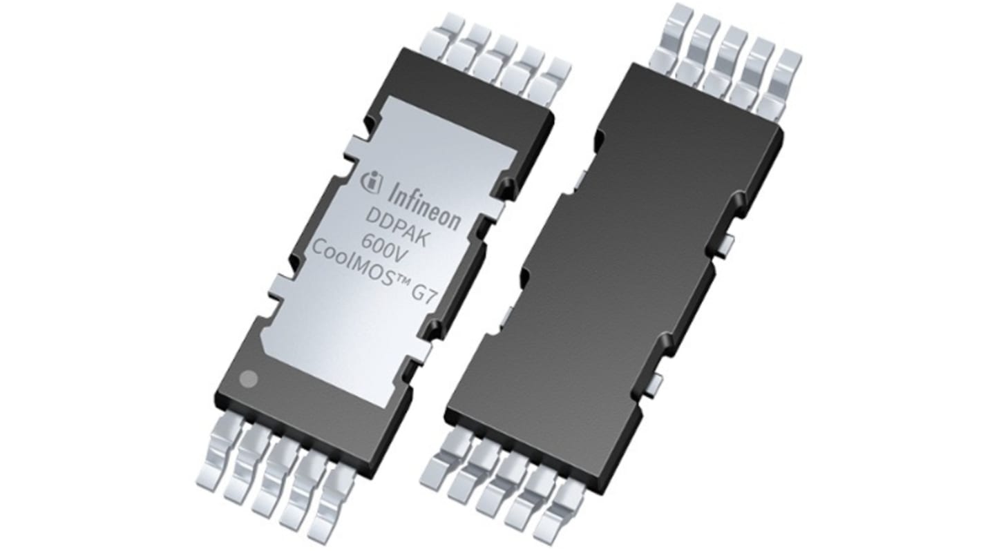
The Infineon technologies introduces Double DPAK (DDPAK), the first top-side cooled surface mount device (SMD) package addressing high power SMPS applications such as PC power, solar, server and telecom. The benefits of the already existing high voltage technology 600V Cool MOS G7 super junction (SJ) MOSFETis combined with the innovative concept of top-side cooling, providing a system solution for high current hard switching topologies such as PFC and a high-end efficiency solution for LLC topologies.
Gives best-in-class FOM RDS(on) x Eoss and RDS(on) x Qg
Innovative top-side cooling concept
Inbuilt 4th pin Kelvin source configuration and low parasitic source inductance
TCOB capability of >> 2.000 cycles, MSL1 compliant and total Pb-free
Enabling highest energy efficiency
Thermal decoupling of board and semiconductor allows to overcome thermal PCB limits
Reduced parasitic source inductance improves e efficiency and ease-of-use
Enables higher power density solutions
Exceeding the highest quality standards
Liens connexes
- Infineon C7 GOLD Type N-Channel MOSFET & Diode 650 V Enhancement, 10-Pin HDSOP IPDD60R080G7XTMA1
- Infineon C7 GOLD Type N-Channel MOSFET & Diode 650 V Enhancement, 10-Pin HDSOP
- Infineon C7 GOLD Type N-Channel MOSFET & Diode 650 V Enhancement, 10-Pin HDSOP IPDD60R150G7XTMA1
- Infineon C7 GOLD Type N-Channel MOSFET 650 V Enhancement, 8-Pin HSOF
- Infineon C7 GOLD Type N-Channel MOSFET 650 V Enhancement, 8-Pin HSOF IPT60R150G7XTMA1
- Infineon CoolMOS C7 Type N-Channel MOSFET 650 V Enhancement, 5-Pin VSON
- Infineon CoolMOS C7 Type N-Channel MOSFET 650 V Enhancement, 5-Pin VSON IPL65R130C7AUMA1
- Infineon CoolMOS C7 Type N-Channel MOSFET 650 V Enhancement, 3-Pin TO-220