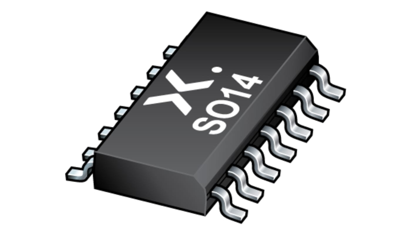
Nexperia 1 Surface Shift Register 74HCT SO, 14-Pin
- N° de stock RS:
- 170-4902
- Référence fabricant:
- 74HCT164D,653
- Fabricant:
- Nexperia

Actuellement indisponible
Nous ne savons pas si cet article sera de nouveau disponible. RS a l'intention de le retirer de son assortiment sous peu.
- N° de stock RS:
- 170-4902
- Référence fabricant:
- 74HCT164D,653
- Fabricant:
- Nexperia
Spécifications
Documentation technique
Législations et de normes
Détails du produit
Recherchez des produits similaires en sélectionnant un ou plusieurs attributs.
Sélectionner tout | Attribut | Valeur |
|---|---|---|
| Marque | Nexperia | |
| Product Type | Shift Register | |
| Package Type | SO | |
| Logic Family | 74HCT | |
| Mount Type | Surface | |
| Number of Elements | 1 | |
| Pin Count | 14 | |
| Minimum Supply Voltage | 4.5V | |
| Maximum Supply Voltage | 5.5V | |
| Trigger Type | Positive Edge | |
| Maximum Operating Temperature | 125°C | |
| Height | 1.75mm | |
| Length | 8.75mm | |
| Standards/Approvals | No | |
| Series | 74HCT164 | |
| Automotive Standard | No | |
| Sélectionner tout | ||
|---|---|---|
Marque Nexperia | ||
Product Type Shift Register | ||
Package Type SO | ||
Logic Family 74HCT | ||
Mount Type Surface | ||
Number of Elements 1 | ||
Pin Count 14 | ||
Minimum Supply Voltage 4.5V | ||
Maximum Supply Voltage 5.5V | ||
Trigger Type Positive Edge | ||
Maximum Operating Temperature 125°C | ||
Height 1.75mm | ||
Length 8.75mm | ||
Standards/Approvals No | ||
Series 74HCT164 | ||
Automotive Standard No | ||
- Pays d'origine :
- TH
The 74HC164: 74HCT164 is an 8-bit serial-in/parallel-out shift register. The device features two serial data inputs (DSA and DSB), eight parallel data outputs (Q0 to Q7). Data is entered serially through DSA or DSB and either input can be used as an Active HIGH enable for data entry through the other input. Data is shifted on the LOW‑to‑HIGH transitions of the clock (CP) input. A LOW on the Master reset input (MR) clears the register and forces all outputs LOW, independently of other inputs. Inputs include clamp diodes. This enables the use of current limiting resistors to Interface inputs to voltages in excess of VCC.
Simple control Interface
I/O expansion
Asynchronous and synchronous load options
High frequency
Cascadable
LED drivers
Displays
Control units