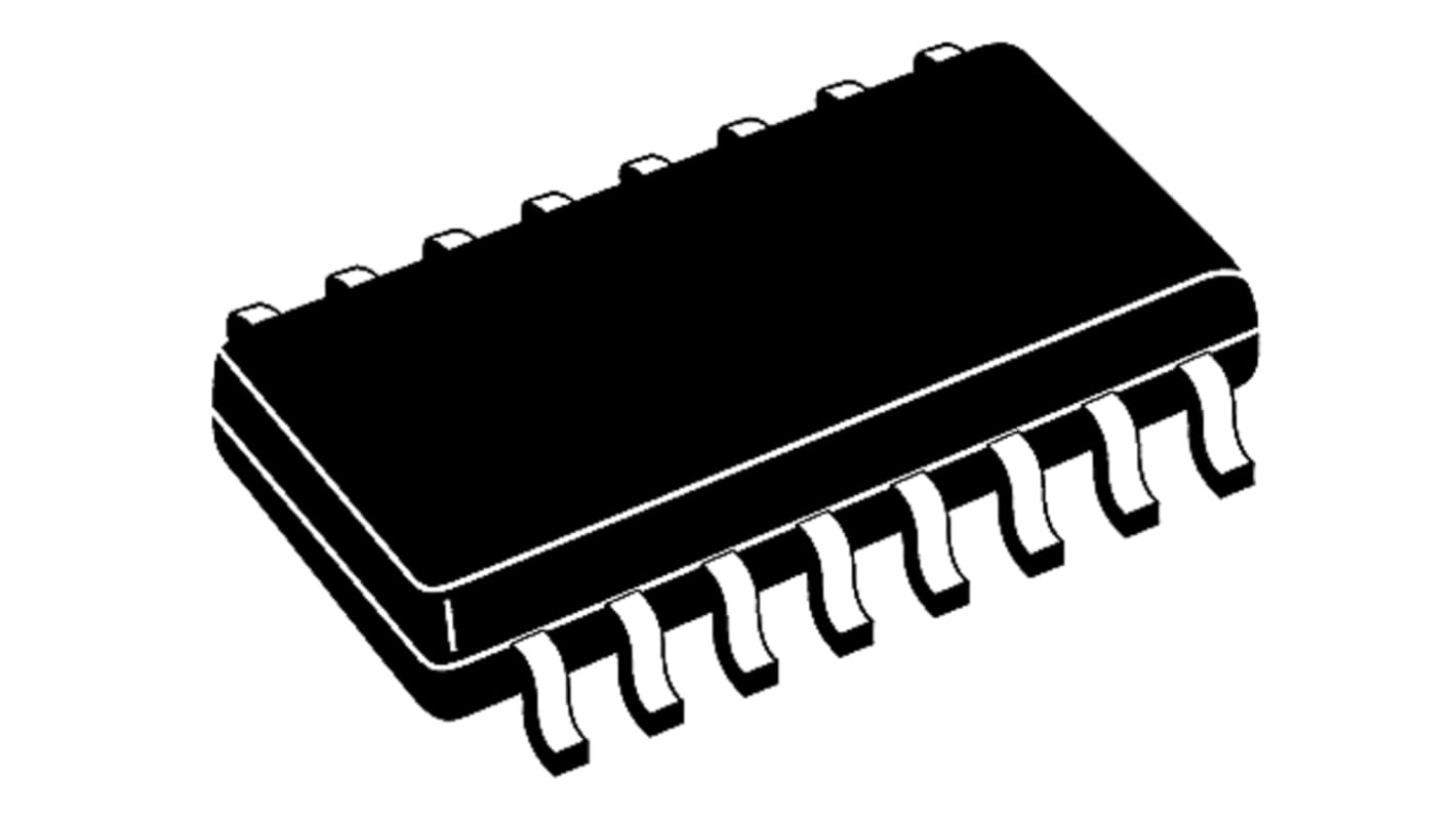
Nexperia 74HC4094D,653 1 Surface Shift Register 74HC SO, 16-Pin
- N° de stock RS:
- 170-7970
- Référence fabricant:
- 74HC4094D,653
- Fabricant:
- Nexperia

Sous-total (1 bobine de 2500 unités)*
500,00 €
(TVA exclue)
600,00 €
(TVA incluse)
Frais de livraison offerts pour toute commande de plus de 90,00 €
Temporairement en rupture de stock
- Expédition à partir du 27 janvier 2027
Besoin de plus? Cliquez sur " Vérifier les dates de livraison " pour plus de détails
Unité | Prix par unité | la bobine* |
|---|---|---|
| 2500 + | 0,20 € | 500,00 € |
*Prix donné à titre indicatif
- N° de stock RS:
- 170-7970
- Référence fabricant:
- 74HC4094D,653
- Fabricant:
- Nexperia
Spécifications
Documentation technique
Législations et de normes
Détails du produit
Recherchez des produits similaires en sélectionnant un ou plusieurs attributs.
Sélectionner tout | Attribut | Valeur |
|---|---|---|
| Marque | Nexperia | |
| Product Type | Shift Register | |
| Package Type | SO | |
| Logic Family | 74HC | |
| Mount Type | Surface | |
| Number of Elements | 1 | |
| Pin Count | 16 | |
| Minimum Supply Voltage | 2V | |
| Maximum Supply Voltage | 6V | |
| Trigger Type | Positive Edge | |
| Maximum Operating Temperature | 125°C | |
| Height | 1.75mm | |
| Standards/Approvals | No | |
| Length | 10mm | |
| Series | 74HC4094 | |
| Automotive Standard | No | |
| Sélectionner tout | ||
|---|---|---|
Marque Nexperia | ||
Product Type Shift Register | ||
Package Type SO | ||
Logic Family 74HC | ||
Mount Type Surface | ||
Number of Elements 1 | ||
Pin Count 16 | ||
Minimum Supply Voltage 2V | ||
Maximum Supply Voltage 6V | ||
Trigger Type Positive Edge | ||
Maximum Operating Temperature 125°C | ||
Height 1.75mm | ||
Standards/Approvals No | ||
Length 10mm | ||
Series 74HC4094 | ||
Automotive Standard No | ||
74HC Family Counters & Shift Registers, Nexperia
A range of 74HC Family CMOS Logic Counters and Shift Registers from NXP. The 74HC Family use silicon gate CMOS technology to achieve operating speeds similar to the LSTTL family but with the low power consumption of standard CMOS integrated circuits.
High-Speed CMOS Logic
Operating Voltage: 2 to 6 V
Compatibility: Input CMOS, Output CMOS