Infineon CoolMOS P6 Type N-Channel MOSFET & Diode, 30 A, 650 V Enhancement, 5-Pin ThinPAK IPL60R360P6SATMA1
- N° de stock RS:
- 220-7435
- Référence fabricant:
- IPL60R360P6SATMA1
- Fabricant:
- Infineon

Offre groupée disponible
Consulter les options de prix de grosSous-total (1 paquet de 10 unités)*
13,56 €
(TVA exclue)
16,41 €
(TVA incluse)
Frais de livraison offerts pour toute commande de plus de 90,00 €
Dernier stock RS
- 5 470 dernière(s) unité(s), prête(s) à l'envoi d'un autre centre de distribution
Unité | Prix par unité | le paquet* |
|---|---|---|
| 10 - 40 | 1,356 € | 13,56 € |
| 50 - 90 | 1,289 € | 12,89 € |
| 100 - 240 | 1,234 € | 12,34 € |
| 250 - 490 | 1,18 € | 11,80 € |
| 500 + | 1,098 € | 10,98 € |
*Prix donné à titre indicatif
- N° de stock RS:
- 220-7435
- Référence fabricant:
- IPL60R360P6SATMA1
- Fabricant:
- Infineon
Spécifications
Documentation technique
Législations et de normes
Détails du produit
Recherchez des produits similaires en sélectionnant un ou plusieurs attributs.
Sélectionner tout | Attribut | Valeur |
|---|---|---|
| Marque | Infineon | |
| Channel Type | Type N | |
| Product Type | MOSFET & Diode | |
| Maximum Continuous Drain Current Id | 30A | |
| Maximum Drain Source Voltage Vds | 650V | |
| Series | CoolMOS P6 | |
| Package Type | ThinPAK | |
| Mount Type | Surface | |
| Pin Count | 5 | |
| Maximum Drain Source Resistance Rds | 360mΩ | |
| Channel Mode | Enhancement | |
| Minimum Operating Temperature | -40°C | |
| Forward Voltage Vf | 0.9V | |
| Typical Gate Charge Qg @ Vgs | 22nC | |
| Maximum Power Dissipation Pd | 89.3W | |
| Maximum Operating Temperature | 150°C | |
| Length | 5.1mm | |
| Standards/Approvals | No | |
| Height | 1.1mm | |
| Automotive Standard | No | |
| Sélectionner tout | ||
|---|---|---|
Marque Infineon | ||
Channel Type Type N | ||
Product Type MOSFET & Diode | ||
Maximum Continuous Drain Current Id 30A | ||
Maximum Drain Source Voltage Vds 650V | ||
Series CoolMOS P6 | ||
Package Type ThinPAK | ||
Mount Type Surface | ||
Pin Count 5 | ||
Maximum Drain Source Resistance Rds 360mΩ | ||
Channel Mode Enhancement | ||
Minimum Operating Temperature -40°C | ||
Forward Voltage Vf 0.9V | ||
Typical Gate Charge Qg @ Vgs 22nC | ||
Maximum Power Dissipation Pd 89.3W | ||
Maximum Operating Temperature 150°C | ||
Length 5.1mm | ||
Standards/Approvals No | ||
Height 1.1mm | ||
Automotive Standard No | ||
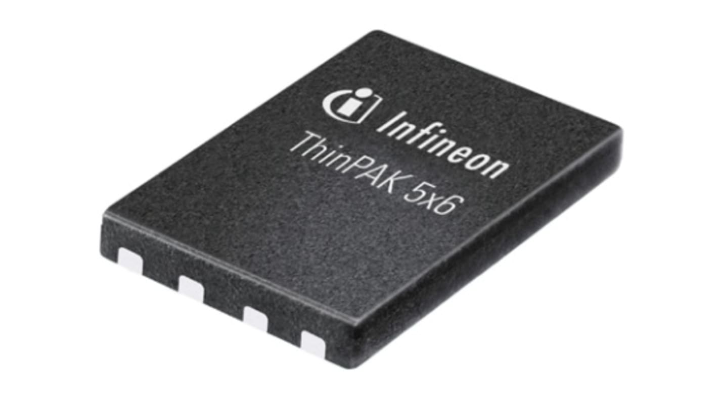
The Infineon new Cool MOS Thin PAK 5x6 is a leadless SMD package especially designed for high voltage MOSFETs. This new package has a very small footprint of 5x6mm 2 and a very low profile with only 1mm height. This significantly smaller package size in combination with its benchmark low parasitic inductances can be used as a new and effective way to decrease system solution size in power- density driven designs. The Thin PAK 5x6 package is characterized by a very low source inductance 1.6nH, as well as a similar thermal performance as DPAK. The package hence enables faster and thus more efficient switching of power MOSFETs and is easier to handle in terms of switching behaviour and EMI.
Extremely low losses due to very low FOMRdson*Qg and Eoss
Very high commutation ruggedness
Easy to use/drive
Pb-freeplating, Halogen free mold compound
Qualified for industrial grade applications according to JEDEC
Liens connexes
- Infineon CoolMOS P6 Type N-Channel MOSFET & Diode 650 V Enhancement, 5-Pin ThinPAK
- Infineon 600V CoolMOS CFD7 Type N-Channel MOSFET 650 V Enhancement, 5-Pin ThinPAK
- Infineon CoolMOS P6 Type N-Channel MOSFET & Diode 650 V Enhancement, 3-Pin TO-220
- Infineon CoolMOS P6 Type N-Channel MOSFET & Diode 650 V Enhancement, 3-Pin TO-247
- Infineon 600V CoolMOS CFD7 Type N-Channel MOSFET 650 V Enhancement, 5-Pin ThinPAK IPL60R185CFD7AUMA1
- Infineon CoolMOS P6 Type N-Channel MOSFET & Diode 650 V Enhancement, 3-Pin TO-220 IPA60R125P6XKSA1
- Infineon CoolMOS P6 Type N-Channel MOSFET & Diode 650 V Enhancement, 3-Pin TO-247 IPW60R099P6XKSA1
- Infineon CoolMOS P6 Type N-Channel MOSFET 650 V Enhancement, 4-Pin TO-220