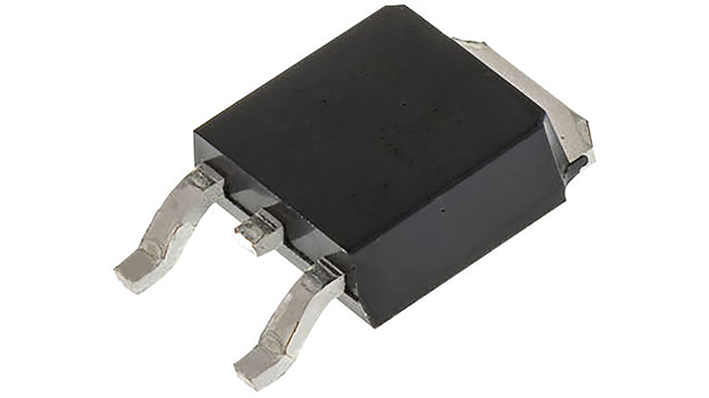
onsemi PowerTrench Type P-Channel MOSFET, 6.7 A, 12 V Enhancement, 3-Pin TO-252 FDD306P
- N° de stock RS:
- 759-9065
- Référence fabricant:
- FDD306P
- Fabricant:
- onsemi

Offre groupée disponible
Consulter les options de prix de grosSous-total (1 paquet de 10 unités)*
8,90 €
(TVA exclue)
10,80 €
(TVA incluse)
Frais de livraison offerts pour toute commande de plus de 90,00 €
En stock
- Plus 2 290 unité(s) expédiée(s) à partir du 20 juillet 2026
Besoin de plus? Cliquez sur " Vérifier les dates de livraison " pour plus de détails
Unité | Prix par unité | le paquet* |
|---|---|---|
| 10 - 90 | 0,89 € | 8,90 € |
| 100 - 240 | 0,768 € | 7,68 € |
| 250 - 490 | 0,666 € | 6,66 € |
| 500 - 990 | 0,584 € | 5,84 € |
| 1000 + | 0,533 € | 5,33 € |
*Prix donné à titre indicatif
- N° de stock RS:
- 759-9065
- Référence fabricant:
- FDD306P
- Fabricant:
- onsemi
Spécifications
Documentation technique
Législations et de normes
Détails du produit
Recherchez des produits similaires en sélectionnant un ou plusieurs attributs.
Sélectionner tout | Attribut | Valeur |
|---|---|---|
| Marque | onsemi | |
| Channel Type | Type P | |
| Product Type | MOSFET | |
| Maximum Continuous Drain Current Id | 6.7A | |
| Maximum Drain Source Voltage Vds | 12V | |
| Package Type | TO-252 | |
| Series | PowerTrench | |
| Mount Type | Surface | |
| Pin Count | 3 | |
| Maximum Drain Source Resistance Rds | 90mΩ | |
| Channel Mode | Enhancement | |
| Minimum Operating Temperature | -55°C | |
| Typical Gate Charge Qg @ Vgs | 15nC | |
| Forward Voltage Vf | -1.2V | |
| Maximum Power Dissipation Pd | 52W | |
| Maximum Operating Temperature | 175°C | |
| Height | 2.39mm | |
| Length | 6.73mm | |
| Standards/Approvals | No | |
| Automotive Standard | No | |
| Sélectionner tout | ||
|---|---|---|
Marque onsemi | ||
Channel Type Type P | ||
Product Type MOSFET | ||
Maximum Continuous Drain Current Id 6.7A | ||
Maximum Drain Source Voltage Vds 12V | ||
Package Type TO-252 | ||
Series PowerTrench | ||
Mount Type Surface | ||
Pin Count 3 | ||
Maximum Drain Source Resistance Rds 90mΩ | ||
Channel Mode Enhancement | ||
Minimum Operating Temperature -55°C | ||
Typical Gate Charge Qg @ Vgs 15nC | ||
Forward Voltage Vf -1.2V | ||
Maximum Power Dissipation Pd 52W | ||
Maximum Operating Temperature 175°C | ||
Height 2.39mm | ||
Length 6.73mm | ||
Standards/Approvals No | ||
Automotive Standard No | ||
PowerTrench® P-Channel MOSFET, Fairchild Semiconductor
PowerTrench® MOSFETs are optimised power switches that offer increase of system efficiency and power density. They combine small gate charge(Qg), small reverse recovery charge(Qrr) and soft reverse recovery body diode, which contributes to fast switching of synchronous rectification in AC/DC power supplies.
The latest PowerTrench® MOSFETs employa shielded-gate structure that provides charge balance. By utilizing this Advanced technology, the FOM (Figure of Merit) of these devices is significant lower than that of previous generations.
Soft body diode performance of the PowerTrench® MOSFETs is able to eliminate snubber circuits or replace a higher voltage rating MOSFET.
MOSFET Transistors, ON Semi
ON Semi offers a substantial portfolio of MOSFET devices that includes high-voltage (>250V) and low-voltage (<250V) types. The Advanced silicon technology provides smaller die sizes, which it is incorporated into multiple industry-standard and thermally-enhanced packages.
ON Semi MOSFETs provide superior design reliability from reduced voltage spikes and overshoot, to lower junction capacitance and reverse recovery charge, to elimination of additional external components to keep systems up and running longer.
Liens connexes
- onsemi PowerTrench Type P-Channel MOSFET 12 V Enhancement, 3-Pin TO-252
- onsemi PowerTrench Type P-Channel MOSFET 40 V Enhancement, 3-Pin TO-252
- onsemi PowerTrench Type P-Channel MOSFET 40 V Enhancement, 3-Pin TO-252 FDD4243
- onsemi PowerTrench Type P-Channel PowerTrench MOSFET 40 V Enhancement, 3-Pin TO-252
- onsemi PowerTrench Type P-Channel PowerTrench MOSFET 40 V Enhancement, 3-Pin TO-252 FDD4141
- onsemi PowerTrench Type P-Channel MOSFET 30 V Enhancement, 3-Pin TO-252
- onsemi PowerTrench Type P-Channel MOSFET 35 V Enhancement, 3-Pin TO-252
- onsemi PowerTrench Type P-Channel MOSFET 40 V Enhancement, 3-Pin TO-252