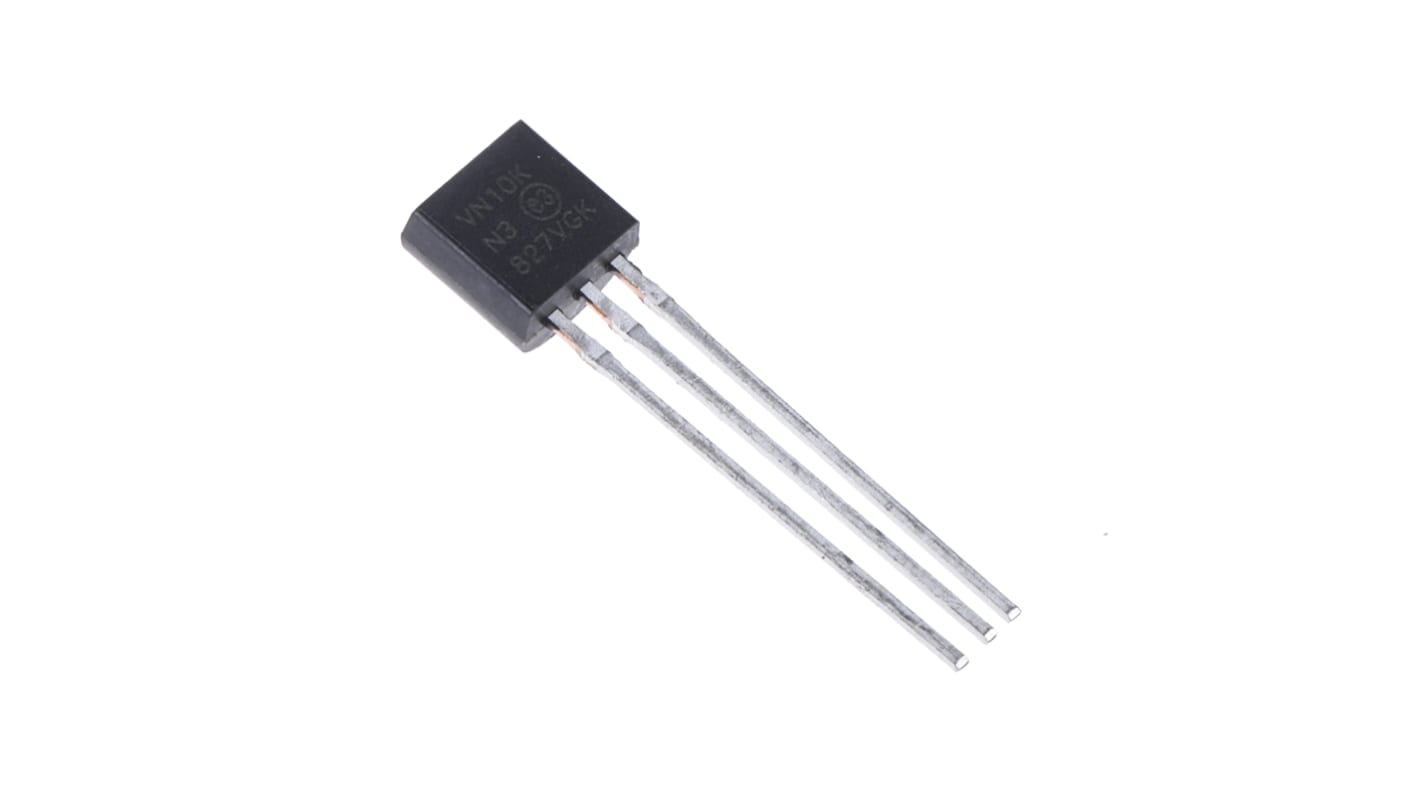
Microchip VN10K Type N-Channel MOSFET, 310 mA, 60 V Enhancement, 3-Pin TO-92 VN10KN3-G
- N° de stock RS:
- 177-9716
- Numéro d'article Distrelec:
- 304-38-572
- Référence fabricant:
- VN10KN3-G
- Fabricant:
- Microchip

Offre groupée disponible
Consulter les options de prix de grosSous-total (1 paquet de 25 unités)*
13,50 €
(TVA exclue)
16,25 €
(TVA incluse)
Frais de livraison offerts pour toute commande de plus de 90,00 €
Stock limité
- Plus 200 unité(s) expédiée(s) à partir du 20 juillet 2026
- Plus 175 unité(s) expédiée(s) à partir du 27 juillet 2026
Besoin de plus? Cliquez sur " Vérifier les dates de livraison " pour plus de détails
Unité | Prix par unité | le paquet* |
|---|---|---|
| 25 - 75 | 0,54 € | 13,50 € |
| 100 + | 0,502 € | 12,55 € |
*Prix donné à titre indicatif
- N° de stock RS:
- 177-9716
- Numéro d'article Distrelec:
- 304-38-572
- Référence fabricant:
- VN10KN3-G
- Fabricant:
- Microchip
Spécifications
Documentation technique
Législations et de normes
Détails du produit
Recherchez des produits similaires en sélectionnant un ou plusieurs attributs.
Sélectionner tout | Attribut | Valeur |
|---|---|---|
| Marque | Microchip | |
| Product Type | MOSFET | |
| Channel Type | Type N | |
| Maximum Continuous Drain Current Id | 310mA | |
| Maximum Drain Source Voltage Vds | 60V | |
| Package Type | TO-92 | |
| Series | VN10K | |
| Mount Type | Through Hole | |
| Pin Count | 3 | |
| Maximum Drain Source Resistance Rds | 7.5Ω | |
| Channel Mode | Enhancement | |
| Forward Voltage Vf | 0.8V | |
| Minimum Operating Temperature | -55°C | |
| Maximum Power Dissipation Pd | 1W | |
| Maximum Operating Temperature | 150°C | |
| Height | 5.33mm | |
| Standards/Approvals | No | |
| Length | 5.08mm | |
| Automotive Standard | No | |
| Sélectionner tout | ||
|---|---|---|
Marque Microchip | ||
Product Type MOSFET | ||
Channel Type Type N | ||
Maximum Continuous Drain Current Id 310mA | ||
Maximum Drain Source Voltage Vds 60V | ||
Package Type TO-92 | ||
Series VN10K | ||
Mount Type Through Hole | ||
Pin Count 3 | ||
Maximum Drain Source Resistance Rds 7.5Ω | ||
Channel Mode Enhancement | ||
Forward Voltage Vf 0.8V | ||
Minimum Operating Temperature -55°C | ||
Maximum Power Dissipation Pd 1W | ||
Maximum Operating Temperature 150°C | ||
Height 5.33mm | ||
Standards/Approvals No | ||
Length 5.08mm | ||
Automotive Standard No | ||
Microchip Technology MOSFET
The Microchip Technology through-hole mount N-channel MOSFET is a new age product with a drain-source resistance of 5ohms at a gate-source voltage of 10V. It has a drain-source voltage of 60V and a maximum gate-source voltage of 30V. It has continuous drain current of 310mA and maximum power dissipation of 1W. The minimum and a maximum driving voltage for this transistor are 5V and 10V respectively. The MOSFET is an enhancement mode (normally off) transistor that utilizes a vertical DMOS structure and well-proven, silicon gate manufacturing process. This combination produces a device with the power handling capabilities of bipolar transistors and the high input impedance and positive temperature coefficient inherent in MOS devices. A significant characteristic of all MOS structures, this device is free from thermal runaway and thermally induced secondary breakdown. This vertical DMOS FET has been optimized for lower switching and conduction losses. The MOSFET offers excellent efficiency along with a long and productive life without compromising performance or functionality.
Features and Benefits
• Ease of paralleling
• Excellent thermal stability
• Free from secondary breakdown
• High input impedance and high gain
• Integral source drain diode
• Low CISS and fast switching speeds
• Low power drive requirement
• Operating temperature ranges between -55°C and 150°C
Applications
• Amplifiers
• Converters
• Drivers (relays, hammers, solenoids, lamps, memories, displays, bipolar transistors, etc.)
• Motor controls
• Power supply circuits
• Switches
Certifications
• ANSI/ESD S20.20:2014
• BS EN 61340-5-1:2007
• JEDEC
Liens connexes
- Microchip VN10K Type N-Channel MOSFET 60 V Enhancement, 3-Pin TO-92
- Microchip Type N-Channel MOSFET 60 V Enhancement, 3-Pin TO-92 VN2222LL-G
- Microchip 2N7000 Type N-Channel MOSFET 60 V Enhancement, 3-Pin TO-92 2N7000-G
- Microchip TN2106 Type N-Channel MOSFET 60 V Enhancement, 3-Pin TO-92 TN2106N3-G
- Microchip Type P-Channel MOSFET 60 V Enhancement, 3-Pin TO-92 VP2106N3-G
- Microchip 2N7008 Type N-Channel MOSFET 60 V Enhancement, 3-Pin TO-92 2N7008-G
- Microchip Type N-Channel MOSFET 60 V Enhancement, 3-Pin TO-92
- Microchip VP2206 Type P-Channel MOSFET -60 V Enhancement, 3-Pin TO-92 VP2206N3-G