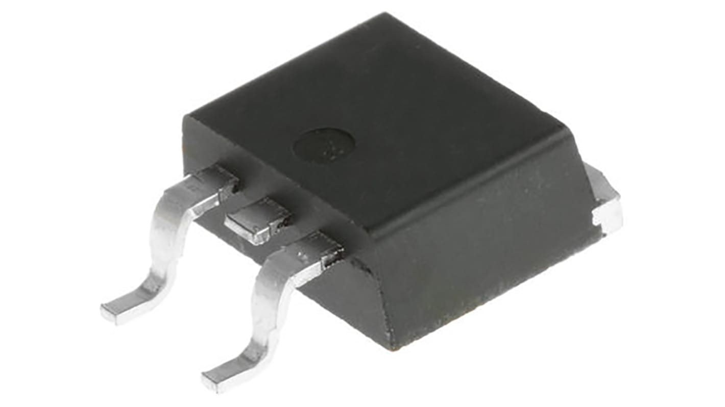
Infineon HEXFET Type N-Channel MOSFET, 43 A, 60 V Enhancement, 3-Pin TO-263
- N° de stock RS:
- 145-9494
- Référence fabricant:
- IRFS3806TRLPBF
- Fabricant:
- Infineon

Offre groupée disponible
Consulter les options de prix de grosSous-total (1 bobine de 800 unités)*
353,60 €
(TVA exclue)
428,00 €
(TVA incluse)
Frais de livraison offerts pour toute commande de plus de 90,00 €
En stock
- Plus 800 unité(s) expédiée(s) à partir du 16 juillet 2026
Besoin de plus? Cliquez sur " Vérifier les dates de livraison " pour plus de détails
Unité | Prix par unité | la bobine* |
|---|---|---|
| 800 - 800 | 0,442 € | 353,60 € |
| 1600 - 1600 | 0,42 € | 336,00 € |
| 2400 + | 0,394 € | 315,20 € |
*Prix donné à titre indicatif
- N° de stock RS:
- 145-9494
- Référence fabricant:
- IRFS3806TRLPBF
- Fabricant:
- Infineon
Spécifications
Documentation technique
Législations et de normes
Détails du produit
Recherchez des produits similaires en sélectionnant un ou plusieurs attributs.
Sélectionner tout | Attribut | Valeur |
|---|---|---|
| Marque | Infineon | |
| Channel Type | Type N | |
| Product Type | MOSFET | |
| Maximum Continuous Drain Current Id | 43A | |
| Maximum Drain Source Voltage Vds | 60V | |
| Series | HEXFET | |
| Package Type | TO-263 | |
| Mount Type | Surface | |
| Pin Count | 3 | |
| Maximum Drain Source Resistance Rds | 15.8mΩ | |
| Channel Mode | Enhancement | |
| Typical Gate Charge Qg @ Vgs | 22nC | |
| Forward Voltage Vf | 1.3V | |
| Maximum Power Dissipation Pd | 71W | |
| Minimum Operating Temperature | -55°C | |
| Maximum Operating Temperature | 175°C | |
| Standards/Approvals | No | |
| Height | 4.83mm | |
| Length | 10.67mm | |
| Automotive Standard | No | |
| Sélectionner tout | ||
|---|---|---|
Marque Infineon | ||
Channel Type Type N | ||
Product Type MOSFET | ||
Maximum Continuous Drain Current Id 43A | ||
Maximum Drain Source Voltage Vds 60V | ||
Series HEXFET | ||
Package Type TO-263 | ||
Mount Type Surface | ||
Pin Count 3 | ||
Maximum Drain Source Resistance Rds 15.8mΩ | ||
Channel Mode Enhancement | ||
Typical Gate Charge Qg @ Vgs 22nC | ||
Forward Voltage Vf 1.3V | ||
Maximum Power Dissipation Pd 71W | ||
Minimum Operating Temperature -55°C | ||
Maximum Operating Temperature 175°C | ||
Standards/Approvals No | ||
Height 4.83mm | ||
Length 10.67mm | ||
Automotive Standard No | ||
- Pays d'origine :
- CN
Infineon HEXFET Series MOSFET, 43A Maximum Continuous Drain Current, 71W Maximum Power Dissipation - IRFS3806TRLPBF
This MOSFET is crafted for optimal performance in high-efficiency applications. Its enhancement mode configuration is pivotal in power management, driving significant usage across diverse electronic systems. It supports efficient switching and signal amplification, essential for sectors such as automation, electronics, and the electrical and mechanical industries.
Features & Benefits
• High continuous drain current capability of up to 43A
• Efficient operation with a maximum drain-source voltage of 60V
• Low on-resistance reduces power loss
• High-temperature application suitability with a range up to +175°C
• Space-saving surface mount design
• Enhanced ruggedness against dynamic stress for consistent performance
Applications
• Ideal for high-speed power switching scenarios
• Used in uninterruptible power supply systems
• Applicable in synchronous rectification within switched-mode power supplies
• Suitable for hard-switched and high-frequency circuits
What is the maximum gate-to-source voltage?
The maximum gate-to-source voltage for this component is -20V to +20V, allowing flexibility in various circuit designs.
How does the on-resistance affect power dissipation?
Lower on-resistance minimises power dissipation during operation, leading to enhanced efficiency and thermal performance.
What is the typical gate charge required?
The typical gate charge at a gate-source voltage of 10V is 22nC, enabling quick switching transitions.
Is it compatible with surface mount PCB designs?
Yes, the surface mount design is suitable for modern PCB layouts, facilitating integration into Compact electronic devices.
What factors should be considered when using the MOSFET in high-temperature applications?
When operating at high temperatures, ensure adequate thermal management is implemented to respect the maximum operating temperature limit of +175°C for reliability.
Liens connexes
- Infineon HEXFET Type N-Channel MOSFET 60 V Enhancement, 3-Pin TO-263 IRFS3806TRLPBF
- Infineon HEXFET Type N-Channel MOSFET 60 V Enhancement, 8-Pin TO-263
- Infineon HEXFET Type N-Channel MOSFET 60 V Enhancement, 3-Pin TO-263
- Infineon HEXFET Type N-Channel MOSFET 60 V Enhancement, 8-Pin TO-263
- Infineon HEXFET Type N-Channel MOSFET 60 V Enhancement, 3-Pin TO-263
- Infineon HEXFET Type N-Channel MOSFET 60 V Enhancement, 3-Pin TO-263
- Infineon HEXFET Type N-Channel MOSFET 200 V TO-263
- Infineon HEXFET Type N-Channel MOSFET 60 V Enhancement, 3-Pin TO-263 IRFS7537TRLPBF