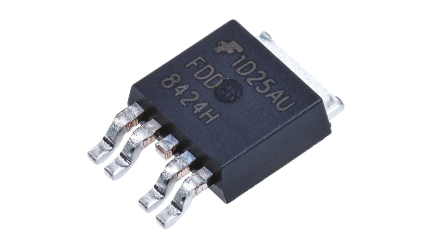
onsemi Common Drain PowerTrench 2 Type N, Type P-Channel MOSFET, 9 A, 40 V Enhancement, 5-Pin TO-252 FDD8424H
- N° de stock RS:
- 124-1698
- Référence fabricant:
- FDD8424H
- Fabricant:
- onsemi

Actuellement indisponible
Nous ne savons pas si cet article sera de nouveau disponible. RS a l'intention de le retirer de son assortiment sous peu.
- N° de stock RS:
- 124-1698
- Référence fabricant:
- FDD8424H
- Fabricant:
- onsemi
Spécifications
Documentation technique
Législations et de normes
Détails du produit
Recherchez des produits similaires en sélectionnant un ou plusieurs attributs.
Sélectionner tout | Attribut | Valeur |
|---|---|---|
| Marque | onsemi | |
| Product Type | MOSFET | |
| Channel Type | Type N, Type P | |
| Maximum Continuous Drain Current Id | 9A | |
| Maximum Drain Source Voltage Vds | 40V | |
| Series | PowerTrench | |
| Package Type | TO-252 | |
| Mount Type | Surface Mount | |
| Pin Count | 5 | |
| Maximum Drain Source Resistance Rds | 54mΩ | |
| Channel Mode | Enhancement | |
| Minimum Operating Temperature | -55°C | |
| Transistor Configuration | Common Drain | |
| Maximum Operating Temperature | 150°C | |
| Length | 6.73mm | |
| Height | 2.39mm | |
| Number of Elements per Chip | 2 | |
| Sélectionner tout | ||
|---|---|---|
Marque onsemi | ||
Product Type MOSFET | ||
Channel Type Type N, Type P | ||
Maximum Continuous Drain Current Id 9A | ||
Maximum Drain Source Voltage Vds 40V | ||
Series PowerTrench | ||
Package Type TO-252 | ||
Mount Type Surface Mount | ||
Pin Count 5 | ||
Maximum Drain Source Resistance Rds 54mΩ | ||
Channel Mode Enhancement | ||
Minimum Operating Temperature -55°C | ||
Transistor Configuration Common Drain | ||
Maximum Operating Temperature 150°C | ||
Length 6.73mm | ||
Height 2.39mm | ||
Number of Elements per Chip 2 | ||
PowerTrench® Dual N/P-Channel MOSFET, Fairchild Semiconductor
PowerTrench® MOSFETs are optimised power switches that offer increase of system efficiency and power density. They combine small gate charge(Qg), small reverse recovery charge(Qrr) and soft reverse recovery body diode, which contributes to fast switching of synchronous rectification in AC/DC power supplies.
The latest PowerTrench® MOSFETs, employ shielded-gate structure that provides charge balance. By utilizing this Advanced technology, the FOM (Figure of Merit) of these devices is significant lower than that of previous generation.
Soft body diode performance of the PowerTrench® MOSFETs is able to eliminate snubber circuit or replace a higher voltage rating MOSFET.
MOSFET Transistors, ON Semi
ON Semi offers a substantial portfolio of MOSFET devices that includes high-voltage (>250V) and low-voltage (<250V) types. The Advanced silicon technology provides smaller die sizes, which it is incorporated into multiple industry-standard and thermally-enhanced packages.
ON Semi MOSFETs provide superior design reliability from reduced voltage spikes and overshoot, to lower junction capacitance and reverse recovery charge, to elimination of additional external components to keep systems up and running longer.
Liens connexes
- onsemi PowerTrench Dual N/P-Channel-Channel MOSFET 9 A 5-Pin DPAK FDD8424H
- onsemi PowerTrench Dual N/P-Channel MOSFET 40 V, 5-Pin DPAK FDD8424H-F085A
- onsemi PowerTrench Dual N/P-Channel MOSFET 6.2 A 8-Pin SOIC FDS4897C
- onsemi PowerTrench Dual N/P-Channel MOSFET 4.5 A 8-Pin SOIC FDS4559-F085
- onsemi Isolated PowerTrench 2 Type P 6.5 A 8-Pin SOIC
- onsemi Isolated PowerTrench 2 Type P 6.5 A 8-Pin SOIC FDS9934C
- onsemi PowerTrench N-Channel MOSFET 100 V, 3-Pin DPAK FDD3682-F085
- onsemi PowerTrench N-Channel MOSFET 40 V, 3-Pin DPAK FDD8444L-F085