Toshiba 74VHC08FT, 4 2-Input AND Logic Gate, 14-Pin TSSOP
- N° de stock RS:
- 171-3594
- Référence fabricant:
- 74VHC08FT
- Fabricant:
- Toshiba

Sous-total (1 paquet de 50 unités)*
12,40 €
(TVA exclue)
15,00 €
(TVA incluse)
Frais de livraison offerts pour toute commande de plus de 90,00 €
En stock
- 7 950 unité(s) prête(s) à être expédiée(s) d'un autre centre de distribution
Besoin de plus? Cliquez sur " Vérifier les dates de livraison " pour plus de détails
Unité | Prix par unité | le paquet* |
|---|---|---|
| 50 + | 0,248 € | 12,40 € |
*Prix donné à titre indicatif
- N° de stock RS:
- 171-3594
- Référence fabricant:
- 74VHC08FT
- Fabricant:
- Toshiba
Spécifications
Documentation technique
Législations et de normes
Détails du produit
Recherchez des produits similaires en sélectionnant un ou plusieurs attributs.
Sélectionner tout | Attribut | Valeur |
|---|---|---|
| Marque | Toshiba | |
| Logic Function | AND | |
| Product Type | Logic Gate | |
| Mount Type | Surface | |
| Number of Elements | 4 | |
| Number of Inputs per Gate | 2 | |
| Schmitt Trigger Input | No | |
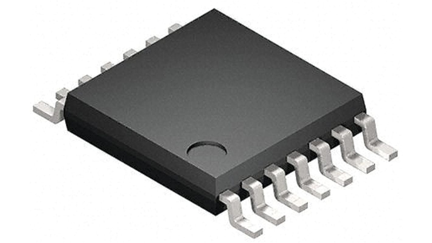
| Package Type | TSSOP | |
| Pin Count | 14 | |
| Logic Family | 74VHC | |
| Input Type | CMOS, TTL | |
| Maximum Propagation Delay Time @ CL | 10ns | |
| Minimum Operating Temperature | -40°C | |
| Maximum High Level Output Current | -8mA | |
| Maximum Operating Temperature | 125°C | |
| Maximum Supply Voltage | 5.5V | |
| Series | 74HC | |
| Standards/Approvals | No | |
| Length | 5mm | |
| Height | 1mm | |
| Minimum Supply Voltage | 2V | |
| Maximum Low Level Output Current | 8mA | |
| Automotive Standard | AEC-Q100 | |
| Output Type | CMOS, Buffer | |
| Sélectionner tout | ||
|---|---|---|
Marque Toshiba | ||
Logic Function AND | ||
Product Type Logic Gate | ||
Mount Type Surface | ||
Number of Elements 4 | ||
Number of Inputs per Gate 2 | ||
Schmitt Trigger Input No | ||
Package Type TSSOP | ||
Pin Count 14 | ||
Logic Family 74VHC | ||
Input Type CMOS, TTL | ||
Maximum Propagation Delay Time @ CL 10ns | ||
Minimum Operating Temperature -40°C | ||
Maximum High Level Output Current -8mA | ||
Maximum Operating Temperature 125°C | ||
Maximum Supply Voltage 5.5V | ||
Series 74HC | ||
Standards/Approvals No | ||
Length 5mm | ||
Height 1mm | ||
Minimum Supply Voltage 2V | ||
Maximum Low Level Output Current 8mA | ||
Automotive Standard AEC-Q100 | ||
Output Type CMOS, Buffer | ||
The 74VHC08FT is an advanced high speed CMOS 2-INPUT AND GATE fabricated with silicon gate C2MOS technology. It achieves the high speed operation similar to equivalent Bipolar Schottky TTL while maintaining the CMOS low power dissipation. The internal circuit is composed of 4 stages including buffer output, which provide high noise immunity and stable output. An input protection circuit ensures that 0 to 5.5 V can be applied to the input pins without regard to the supply voltage. This device can be used to interface 5 V to 3 V systems and two supply systems such as battery back up. This circuit prevents device destruction due to mismatched supply and input voltages
Wide operating temperature: Topr = -40 to 125
High speed: Propagation delay time = 3.8 ns (typ.) at VCC = 5.0 V
Low power dissipation: ICC = 2.0 μA (max) at Ta = 25
High noise immunity: VNIH = VNIL = 28 % VCC (min)
Power-down protection is provided on all inputs.
Balanced propagation delays: tPLH ≈ tPHL
Wide operating voltage range: VCC(opr) = 2.0 to 5.5 V
Low noise: V = 0.8 V (max)