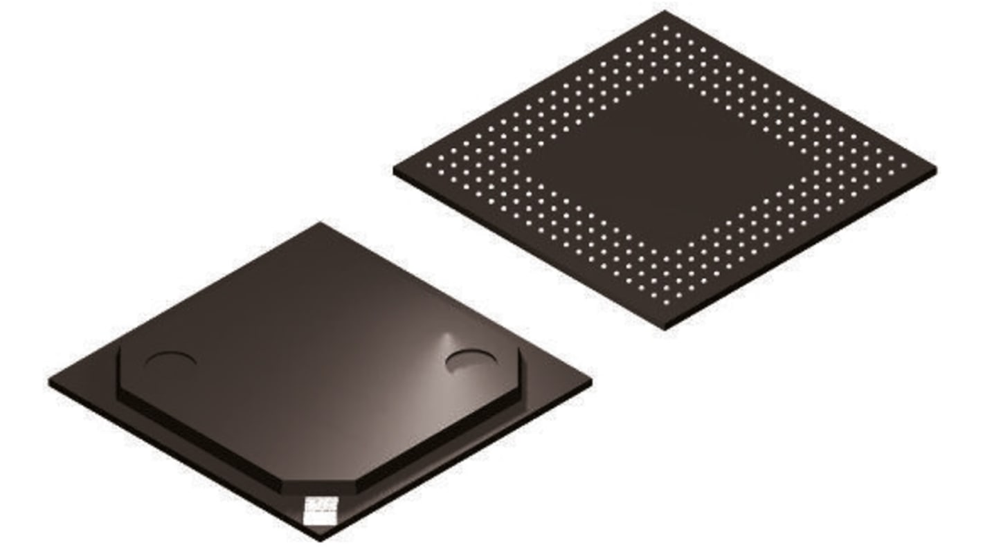
Altera FPGA 5CEBA2F17C8N 5CEBA2 25000 Cells, 25000 Gates, 2002944 bit 9434 Blocks, 256-Pin FBGA
- N° de stock RS:
- 830-3540
- Référence fabricant:
- 5CEBA2F17C8N
- Fabricant:
- Altera

Actuellement indisponible
Nous ne savons pas si cet article sera de nouveau disponible. RS a l'intention de le retirer de son assortiment sous peu.
- N° de stock RS:
- 830-3540
- Référence fabricant:
- 5CEBA2F17C8N
- Fabricant:
- Altera
Spécifications
Documentation technique
Législations et de normes
Détails du produit
Recherchez des produits similaires en sélectionnant un ou plusieurs attributs.
Sélectionner tout | Attribut | Valeur |
|---|---|---|
| Marque | Altera | |
| Series | 5CEBA2 | |
| Product Type | FPGA | |
| Number of Logic Gates | 25000 | |
| Number of Logic Cells | 25000 | |
| Number of Logic Units | 9434 | |
| Number of Registers | 37736 | |
| Number of Multipliers | 50 (18 x 18) | |
| Mount Type | Surface | |
| Package Type | FBGA | |
| Minimum Supply Voltage | 1.07V | |
| Pin Count | 256 | |
| Maximum Supply Voltage | 1.13V | |
| Minimum Operating Temperature | 0°C | |
| Number of RAM Bits | 2002944bit | |
| Maximum Operating Temperature | 85°C | |
| Length | 17mm | |
| Standards/Approvals | No | |
| Automotive Standard | No | |
| Sélectionner tout | ||
|---|---|---|
Marque Altera | ||
Series 5CEBA2 | ||
Product Type FPGA | ||
Number of Logic Gates 25000 | ||
Number of Logic Cells 25000 | ||
Number of Logic Units 9434 | ||
Number of Registers 37736 | ||
Number of Multipliers 50 (18 x 18) | ||
Mount Type Surface | ||
Package Type FBGA | ||
Minimum Supply Voltage 1.07V | ||
Pin Count 256 | ||
Maximum Supply Voltage 1.13V | ||
Minimum Operating Temperature 0°C | ||
Number of RAM Bits 2002944bit | ||
Maximum Operating Temperature 85°C | ||
Length 17mm | ||
Standards/Approvals No | ||
Automotive Standard No | ||
Cyclone FPGA, Altera
An FPGA is a semiconductor device consisting of a matrix of Configurable Logic Blocks (CLBs) connected through programmable interconnects. The user determines these interconnections by programming SRAM. A CLB can be simple (AND, OR gates, etc) or complex (a block of RAM). The FPGA allows changes to be made to a design even after the device is soldered into a PCB.
Liens connexes
- Altera FPGA 5CEBA2 25000 Cells 2002944 bit 9434 Blocks, 256-Pin FBGA
- Altera FPGA EP1C6F256I7N 5980 Blocks, 256-Pin FBGA
- Altera FPGA 5CEBA4 49000 Cells 3464192 bit 18480 Blocks, 256-Pin FBGA
- Altera FPGA Cyclone III 15408 Cells 484-Pin FBGA
- Altera FPGA 5CEBA4F17C8N 5CEBA4 49000 Cells 3464192 bit 18480 Blocks, 256-Pin FBGA
- Altera FPGA EP3C16F484C8N Cyclone III 15408 Cells 484-Pin FBGA
- Altera FPGA Cyclone IV 6272 Cells 276480 bit 392 Blocks, 256-Pin FBGA
- Altera FPGA EP4CE6F17C8N Cyclone IV 6272 Cells 276480 bit 392 Blocks, 256-Pin FBGA