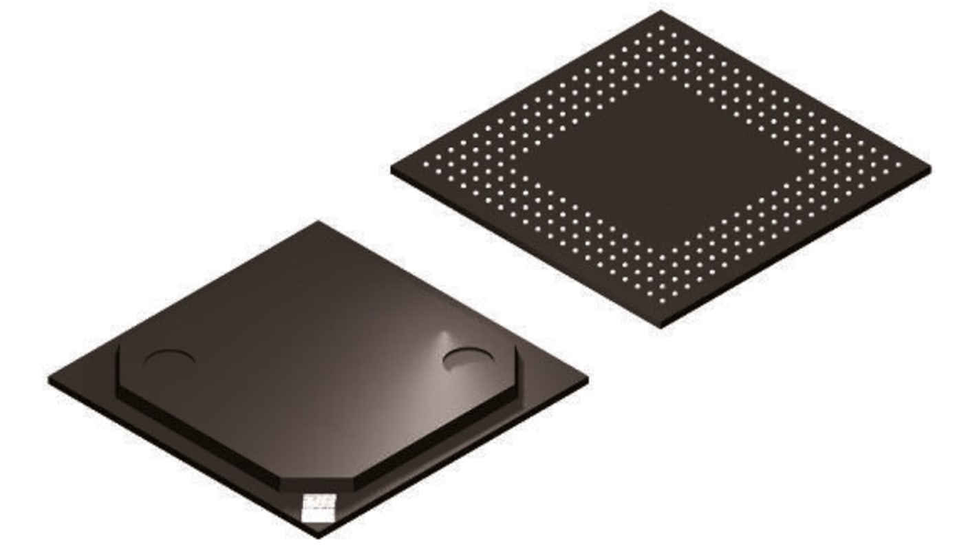
Altera FPGA Cyclone IV 6272 Cells, 6272 Gates, 276480 bit 392 Blocks, 256-Pin FBGA
- N° de stock RS:
- 170-2982
- Référence fabricant:
- EP4CE6F17C8N
- Fabricant:
- Altera

Informations sur le stock actuellement non accessibles
- N° de stock RS:
- 170-2982
- Référence fabricant:
- EP4CE6F17C8N
- Fabricant:
- Altera
Spécifications
Documentation technique
Législations et de normes
Détails du produit
Recherchez des produits similaires en sélectionnant un ou plusieurs attributs.
Sélectionner tout | Attribut | Valeur |
|---|---|---|
| Marque | Altera | |
| Product Type | FPGA | |
| Series | Cyclone IV | |
| Number of Logic Gates | 6272 | |
| Number of Logic Cells | 6272 | |
| Number of Logic Units | 392 | |
| Number of Multipliers | 360 (18 x 18) | |
| Mount Type | Surface | |
| Minimum Supply Voltage | 1.15V | |
| Package Type | FBGA | |
| Pin Count | 256 | |
| Maximum Supply Voltage | 1.25V | |
| Minimum Operating Temperature | 0°C | |
| Number of RAM Bits | 276480bit | |
| Maximum Operating Temperature | 85°C | |
| Standards/Approvals | ISO 9001:2008 | |
| Length | 17mm | |
| Automotive Standard | No | |
| Sélectionner tout | ||
|---|---|---|
Marque Altera | ||
Product Type FPGA | ||
Series Cyclone IV | ||
Number of Logic Gates 6272 | ||
Number of Logic Cells 6272 | ||
Number of Logic Units 392 | ||
Number of Multipliers 360 (18 x 18) | ||
Mount Type Surface | ||
Minimum Supply Voltage 1.15V | ||
Package Type FBGA | ||
Pin Count 256 | ||
Maximum Supply Voltage 1.25V | ||
Minimum Operating Temperature 0°C | ||
Number of RAM Bits 276480bit | ||
Maximum Operating Temperature 85°C | ||
Standards/Approvals ISO 9001:2008 | ||
Length 17mm | ||
Automotive Standard No | ||
- Pays d'origine :
- US
Cyclone FPGA, Altera
An FPGA is a semiconductor device consisting of a Matrix of Configurable Logic Blocks (CLBs) connected through programmable interconnects. The user determines these interconnections by programming SRAM. A CLB can be simple (AND, OR gates, etc) or complex (a Block of RAM). The FPGA allows changes to be MADE to a design even after the device is soldered into a PCB.
Liens connexes
- Altera FPGA EP4CE6F17C8N Cyclone IV 6272 Cells 276480 bit 392 Blocks, 256-Pin FBGA
- Altera FPGA Cyclone IV E 6272 Cells 276480 bit 392 Blocks, 256-Pin FBGA
- Altera FPGA EP4CE6F17C8LN Cyclone IV E 6272 Cells 276480 bit 392 Blocks, 256-Pin FBGA
- Altera FPGA Cyclone IV E 6272 Cells 276480 bit 392 Blocks, 144-Pin EQFP
- Altera FPGA EP4CE6E22I7N Cyclone IV E 6272 Cells 276480 bit 392 Blocks, 144-Pin EQFP
- Altera FPGA Cyclone IV 6272 Cells 144-Pin EQFP
- Altera FPGA EP4CE6E22C8N Cyclone IV 6272 Cells 144-Pin EQFP
- Altera FPGA Cyclone IV 28848 Cells 484-Pin FBGA