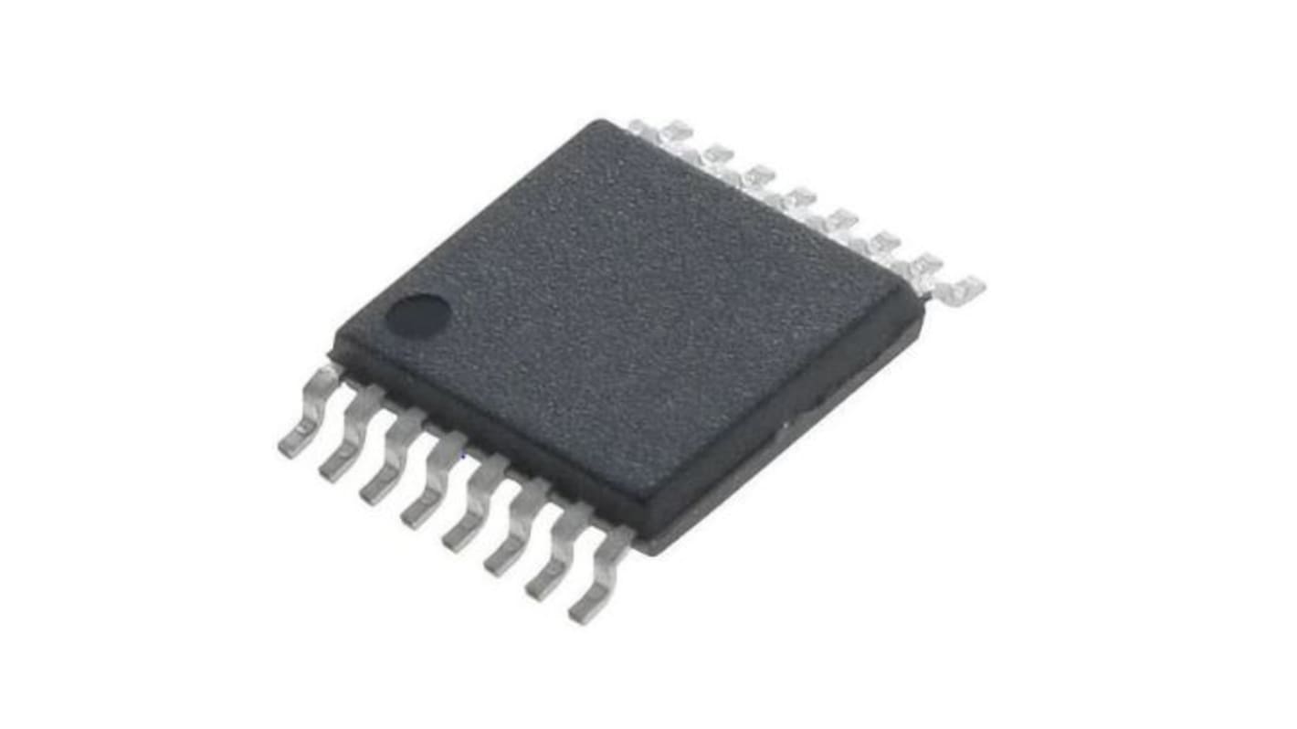
Renesas Electronics 8305AGILF Clock Buffer, 16-Pin 4 TSSOP
- N° de stock RS:
- 216-6204
- Référence fabricant:
- 8305AGILF
- Fabricant:
- Renesas Electronics

Actuellement indisponible
Nous ne savons pas si cet article sera de nouveau disponible. RS a l'intention de le retirer de son assortiment sous peu.
- N° de stock RS:
- 216-6204
- Référence fabricant:
- 8305AGILF
- Fabricant:
- Renesas Electronics
Spécifications
Documentation technique
Législations et de normes
Détails du produit
Recherchez des produits similaires en sélectionnant un ou plusieurs attributs.
Sélectionner tout | Attribut | Valeur |
|---|---|---|
| Marque | Renesas Electronics | |
| Product Type | Clock Buffer | |
| Mount Type | Surface | |
| Package Type | TSSOP | |
| Minimum Supply Voltage | 1.8V | |
| Pin Count | 16 | |
| Maximum Supply Voltage | 3.3V | |
| Minimum Operating Temperature | -40°C | |
| Maximum Operating Temperature | 85°C | |
| Series | 8305A | |
| Length | 4.9mm | |
| Height | 1.2mm | |
| Standards/Approvals | No | |
| Automotive Standard | No | |
| Sélectionner tout | ||
|---|---|---|
Marque Renesas Electronics | ||
Product Type Clock Buffer | ||
Mount Type Surface | ||
Package Type TSSOP | ||
Minimum Supply Voltage 1.8V | ||
Pin Count 16 | ||
Maximum Supply Voltage 3.3V | ||
Minimum Operating Temperature -40°C | ||
Maximum Operating Temperature 85°C | ||
Series 8305A | ||
Length 4.9mm | ||
Height 1.2mm | ||
Standards/Approvals No | ||
Automotive Standard No | ||
The Renesas Electronics ICS8305I is a low skew, 1-to-4, Differential/LVCMOS-toLVCMOS/LVTTL Fanout Buffer. The ICS8305I has selectable clock inputs that accept either differential or single ended input levels. The clock enable is internally synchronized to eliminate runt pulses on the outputs during asynchronous assertion/deassertion of the clock enable pin. Outputs are forced LOW when the clock is disabled. A separate output enable pin controls whether the outputs are in the active or high impedance state.
4 LVCMOS/LVTTL outputs
Selectable differential or LVCMOS/LVTTL clock inputs
CLK, nCLK pair can accept the following differential
input levels: LVPECL, LVDS, LVHSTL, HCSL, SSTL
LVCMOS_CLK supports the following input types:
LVCMOS, LVTTL
Maximum output frequency: 350MHz
Output skew: 40ps (maximum)
Part-to-part skew: 700ps (maximum)
Additive phase jitter, RMS: 0.04ps (typical)
3.3V core, 3.3V, 2.5V or 1.8V output operating supply
-40°C to 85°C ambient operating temperature
Lead-Free package fully RoHS compliant
Liens connexes
- Renesas Electronics 8305AGILF Clock Buffer, 16-Pin 4 TSSOP
- Renesas Electronics 8305AGLF Clock Buffer, 16-Pin 4 TSSOP
- Renesas Electronics 85102AGILF Clock Buffer, 16-Pin 7 TSSOP
- Renesas Electronics 5PB1108PGGI8 Clock Buffer 16-Pin TSSOP-16
- Renesas Electronics 5PB1108PGGK Clock Buffer 16-Pin TSSOP
- Renesas Electronics 5PB1104PGGI Clock Buffer, 8-Pin 4 TSSOP
- Renesas Electronics 85104AGILF Clock Buffer, 20-Pin 4 TSSOP
- Renesas Electronics 2309-1HPGGI Clock Buffer 16-Pin TSSOP