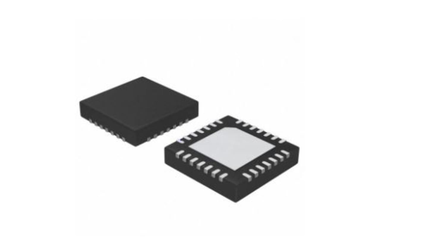
Renesas Electronics 5T9306NLGI Clock Buffer, 8-Pin 6 SOIC
- N° de stock RS:
- 216-6188
- Référence fabricant:
- 5T9306NLGI
- Fabricant:
- Renesas Electronics

Informations sur le stock actuellement non accessibles
- N° de stock RS:
- 216-6188
- Référence fabricant:
- 5T9306NLGI
- Fabricant:
- Renesas Electronics
Spécifications
Documentation technique
Législations et de normes
Détails du produit
Recherchez des produits similaires en sélectionnant un ou plusieurs attributs.
Sélectionner tout | Attribut | Valeur |
|---|---|---|
| Marque | Renesas Electronics | |
| Product Type | Clock Buffer | |
| Mount Type | Surface | |
| Package Type | SOIC | |
| Pin Count | 8 | |
| Minimum Supply Voltage | 2.3V | |
| Maximum Supply Voltage | 2.7V | |
| Minimum Operating Temperature | -40°C | |
| Maximum Operating Temperature | 85°C | |
| Standards/Approvals | No | |
| Height | 0.8mm | |
| Length | 6mm | |
| Series | 5T9306 | |
| Automotive Standard | No | |
| Maximum Output Frequency | 1GHz | |
| Sélectionner tout | ||
|---|---|---|
Marque Renesas Electronics | ||
Product Type Clock Buffer | ||
Mount Type Surface | ||
Package Type SOIC | ||
Pin Count 8 | ||
Minimum Supply Voltage 2.3V | ||
Maximum Supply Voltage 2.7V | ||
Minimum Operating Temperature -40°C | ||
Maximum Operating Temperature 85°C | ||
Standards/Approvals No | ||
Height 0.8mm | ||
Length 6mm | ||
Series 5T9306 | ||
Automotive Standard No | ||
Maximum Output Frequency 1GHz | ||
The Renesas Electronics IDT5T9306 2.5V differential clock buffer is a user-selectable differential input to six LVDS outputs. The fanout from a differential input to six LVDS outputs reduces loading on the preceding driver and provides an efficient clock distribution network. The IDT5T9306 can act as a translator from a differential HSTL, eHSTL, LVEPECL (2.5V), LVPECL (3.3V), CML, or LVDS input to LVDS outputs. A single-ended 3.3V / 2.5V LVTTL input can also be used to translate to LVDS outputs.
Guaranteed Low Skew < 40ps (max)
Very low duty cycle distortion < 125ps (max)
High speed propagation delay < 1.75ns (max)
Additive phase jitter, RMS 0.159ps (typical) @ 125MHz
Up to 1GHz operation
Selectable inputs
Hot insertable and over-voltage tolerant inputs
3.3V / 2.5V LVTTL, HSTL, eHSTL, LVEPECL (2.5V), LVPECL
(3.3V), CML, or LVDS input interface
Selectable differential inputs to six LVDS outputs
Power-down mode
2.5V VDD
Available in VFQFPN package
Liens connexes
- Renesas Electronics 5T9306NLGI Clock Buffer, 8-Pin 6 SOIC
- Renesas Electronics 854S006AGILF Clock Buffer, 24-Pin 6 SOIC
- Renesas Electronics 74FCT38072DCGI Clock Buffer, 8-Pin SOIC
- Renesas Electronics 524MILF Clock Buffer, 8-Pin 4 SOIC
- Renesas Electronics 553MILFT Clock Buffer, 8-Pin 4 SOIC
- Renesas Electronics 553SCMGI Clock Buffer, 8-Pin 4 SOIC
- Renesas Electronics 551MLFT Clock Buffer, 8-Pin 4 SOIC
- Renesas Electronics 74FCT38074SDCGI Clock Buffer, 8-Pin 4 SOIC