Infineon SRAM, CY7C1021D-10VXI- 1 MB
- N° de stock RS:
- 194-8912
- Référence fabricant:
- CY7C1021D-10VXI
- Fabricant:
- Infineon

Actuellement indisponible
Nous ne savons pas si cet article sera de nouveau disponible. RS a l'intention de le retirer de son assortiment sous peu.
- N° de stock RS:
- 194-8912
- Référence fabricant:
- CY7C1021D-10VXI
- Fabricant:
- Infineon
Spécifications
Documentation technique
Législations et de normes
Détails du produit
Recherchez des produits similaires en sélectionnant un ou plusieurs attributs.
Sélectionner tout | Attribut | Valeur |
|---|---|---|
| Marque | Infineon | |
| Product Type | SRAM | |
| Memory Size | 1MB | |
| Number of Words | 64K | |
| Number of Bits per Word | 16 | |
| Maximum Random Access Time | 10ns | |
| Timing Type | Asynchronous | |
| Minimum Supply Voltage | 5V | |
| Maximum Supply Voltage | 3.6V | |
| Mount Type | Through Hole | |
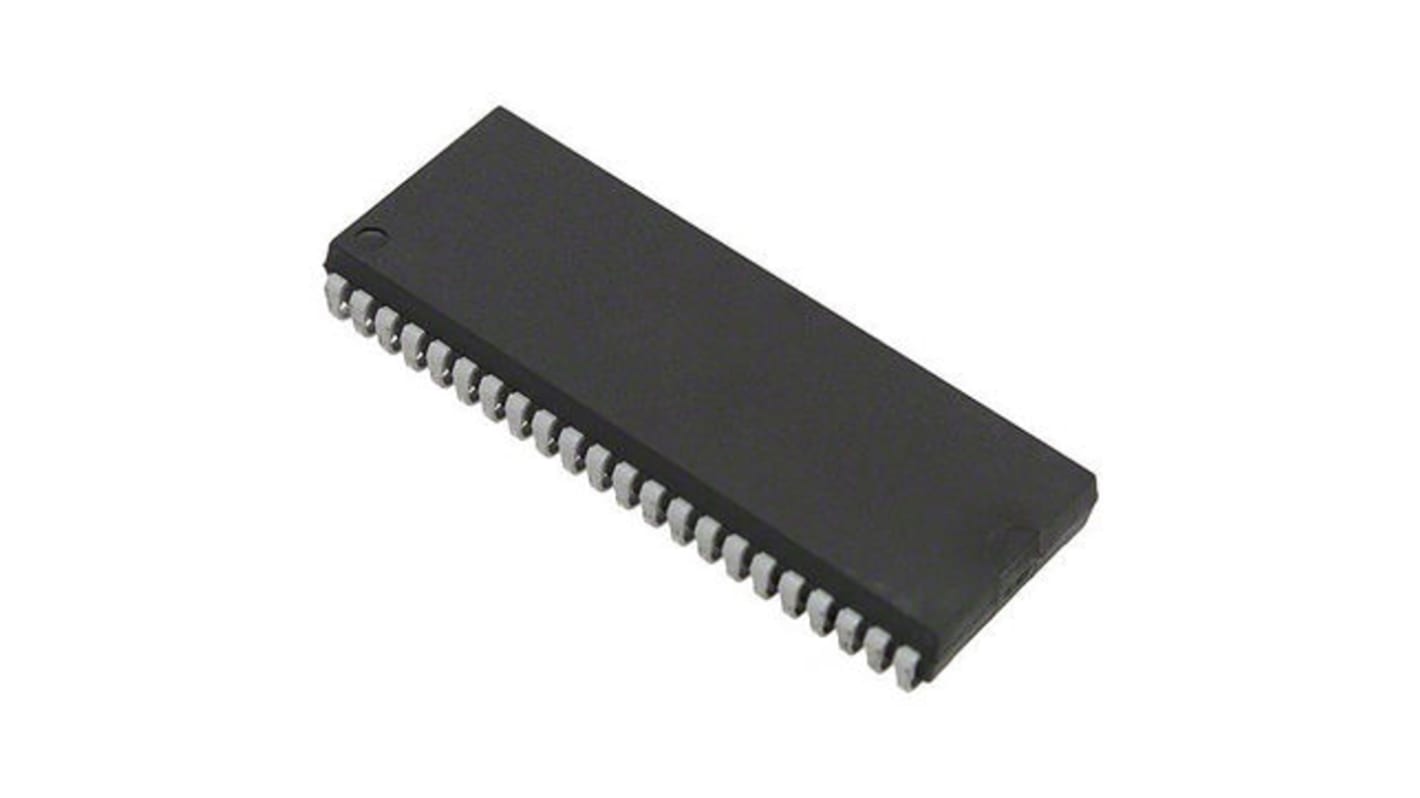
| Package Type | SOJ | |
| Minimum Operating Temperature | -40°C | |
| Maximum Operating Temperature | 85°C | |
| Pin Count | 44 | |
| Length | 28.7mm | |
| Standards/Approvals | RoHS | |
| Height | 3.05mm | |
| Sélectionner tout | ||
|---|---|---|
Marque Infineon | ||
Product Type SRAM | ||
Memory Size 1MB | ||
Number of Words 64K | ||
Number of Bits per Word 16 | ||
Maximum Random Access Time 10ns | ||
Timing Type Asynchronous | ||
Minimum Supply Voltage 5V | ||
Maximum Supply Voltage 3.6V | ||
Mount Type Through Hole | ||
Package Type SOJ | ||
Minimum Operating Temperature -40°C | ||
Maximum Operating Temperature 85°C | ||
Pin Count 44 | ||
Length 28.7mm | ||
Standards/Approvals RoHS | ||
Height 3.05mm | ||
This device has an automatic power down feature that significantly reduces power consumption when deselected. The input and output pins (I/O0 through I/O15) are placed in a high impedance state when the device is deselected (CE HIGH), outputs are disabled (OE HIGH), BHE and BLE are disabled (BHE, BLE HIGH), or during a write operation (CE LOW and WE LOW). Write to the device by taking Chip Enable (CE) and Write Enable (WE) inputs LOW. If Byte Low Enable (BLE) is LOW, then data from I/O pins (I/O0 through I/O7), is written into the location specified on the address pins (A0 through A15). If Byte High Enable (BHE) is LOW, then data from I/O pins (I/O8 through I/O15) is written into the location specified on the address pins (A0 through A15). Read from the device by taking Chip Enable (CE) and Output Enable (OE) LOW while forcing the Write Enable (WE) HIGH. If Byte Low Enable (BLE) is LOW, then data from the memory location specified by the address pins appears on I/O0 to I/O7.