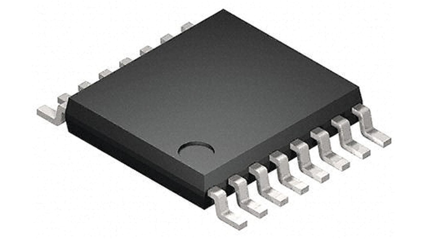
Toshiba, 27 Dual Monostable Multivibrator 74VHC 8 mA, 16-Pin TSSOP
- N° de stock RS:
- 171-3330
- Référence fabricant:
- 74VHC221AFT
- Fabricant:
- Toshiba

Sous-total (1 bobine de 2500 unités)*
270,00 €
(TVA exclue)
327,50 €
(TVA incluse)
Frais de livraison offerts pour toute commande de plus de 90,00 €
Temporairement en rupture de stock
- Expédition à partir du 27 novembre 2026
Besoin de plus? Cliquez sur " Vérifier les dates de livraison " pour plus de détails
Unité | Prix par unité | la bobine* |
|---|---|---|
| 2500 + | 0,108 € | 270,00 € |
*Prix donné à titre indicatif
- N° de stock RS:
- 171-3330
- Référence fabricant:
- 74VHC221AFT
- Fabricant:
- Toshiba
Spécifications
Documentation technique
Législations et de normes
Détails du produit
Recherchez des produits similaires en sélectionnant un ou plusieurs attributs.
Sélectionner tout | Attribut | Valeur |
|---|---|---|
| Marque | Toshiba | |
| Product Type | Dual Monostable Multivibrator | |
| Logic Family | 74VHC | |
| Number of Elements per Chip | 27 | |
| Maximum High Level Output Current | -8mA | |
| Maximum Low Level Output Current | 8mA | |
| Minimum Pulse Width | 5ns | |
| Maximum Quiescent Current | 80μA | |
| Mount Type | Surface | |
| Minimum Supply Voltage | 2V | |
| Package Type | TSSOP | |
| Maximum Supply Voltage | 5.5V | |
| Multivibrator Type | Monostable Multivibrator | |
| Minimum Operating Temperature | -40°C | |
| Maximum Propagation Delay Time @ CL | 8.1ns | |
| Pin Count | 16 | |
| Maximum Operating Temperature | 125°C | |
| Standards/Approvals | No | |
| Series | 74VHC221AFT | |
| Length | 5mm | |
| Height | 1mm | |
| Automotive Standard | AEC-Q100 | |
| Sélectionner tout | ||
|---|---|---|
Marque Toshiba | ||
Product Type Dual Monostable Multivibrator | ||
Logic Family 74VHC | ||
Number of Elements per Chip 27 | ||
Maximum High Level Output Current -8mA | ||
Maximum Low Level Output Current 8mA | ||
Minimum Pulse Width 5ns | ||
Maximum Quiescent Current 80μA | ||
Mount Type Surface | ||
Minimum Supply Voltage 2V | ||
Package Type TSSOP | ||
Maximum Supply Voltage 5.5V | ||
Multivibrator Type Monostable Multivibrator | ||
Minimum Operating Temperature -40°C | ||
Maximum Propagation Delay Time @ CL 8.1ns | ||
Pin Count 16 | ||
Maximum Operating Temperature 125°C | ||
Standards/Approvals No | ||
Series 74VHC221AFT | ||
Length 5mm | ||
Height 1mm | ||
Automotive Standard AEC-Q100 | ||
The 74VHC123A/221AFT are high speed CMOS MONOSTABLE MULTIVIBRATOR fabricated with silicon gate C2MOS technology. There are two trigger inputs, A input (negative edge), and B input (positive edge). These inputs are valid for a slow rise/fall time signal (tr = tf = 1 s) as they are schmitt trigger inputs. This device may also be triggered by using CLR input (positive edge).After triggering, the output stays in a MONOSTABLE state for a time period determined by the external resistor and capacitor (RX, CX). A low level at the CLR input breaks this state. Limits for CX and RX are:External capacitor, CX: No limit External resistor, RX: VCC = 2.0 V more than 5 kΩ CC ≥ 3.0 V more than 1 kΩ An input protection circuit ensures that 0 to 5.5 V can be applied to the input pins without regard to the supply voltage. This device can be used to interface 5 V to 3 V systems and two supply systems such as battery back up. This circuit prevents device destruction due to mismatched supply and input voltages
Wide operating temperature range: Topr = -40 to 125
High speed: Propagation delay time = 8.1 ns (typ.) at VCC = 5 V
Low power dissipation:
Standby state: 4.0 μA (max) at Ta = 25
Active state: 750 μA (max) at Ta = 25
High noise immunity: VNIH = VNIL = 28 % VCC (min)
Power-down protection is provided on all inputs.
Balanced propagation delays: tPLH ≈ tPHL
Wide operating voltage range: VCC(opr) = 2.0 V to 5.5 V
Pin and function compatible with 74HC123,74HC221 type
Liens connexes
- Toshiba 74VHC221AFT 16-Pin TSSOP
- Toshiba 16-Pin TSSOP
- Toshiba 74VHC123AFT 16-Pin TSSOP
- Nexperia 16-Pin TSSOP
- Nexperia 16-Pin TSSOP
- Nexperia 16-Pin TSSOP
- Nexperia 74HC4538PW 2 Dual Monostable Multivibrator HC 5.2 mA, 16-Pin TSSOP
- Nexperia 74HC123PW-Q100 2 Dual Monostable Multivibrator 74HC 5.2 mA, 16-Pin TSSOP