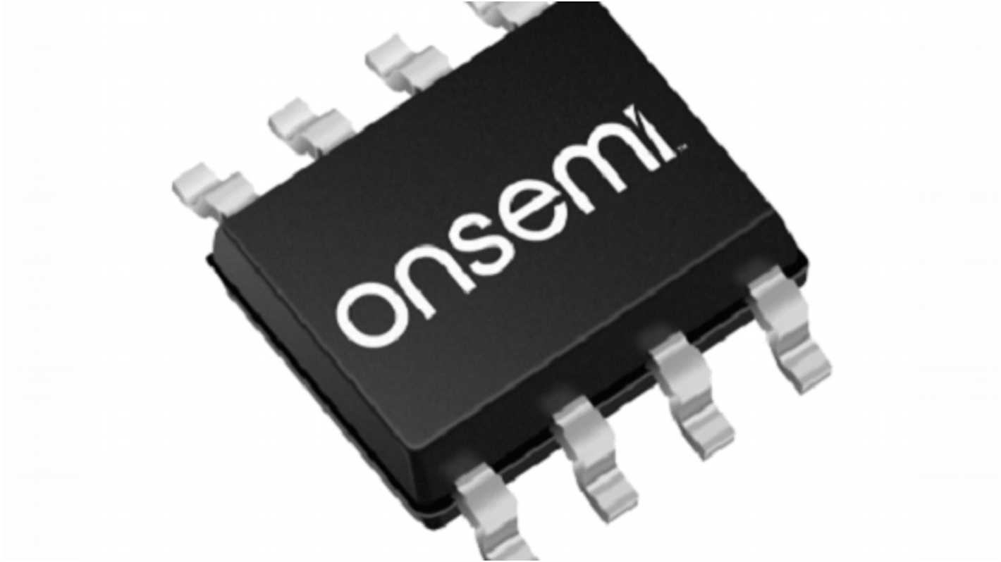
onsemi NCV57091BDWR2G MOSFET Gate Driver, 6.5 A 8-Pin 22 V, SOIC
- N° de stock RS:
- 244-9171
- Référence fabricant:
- NCV57091BDWR2G
- Fabricant:
- onsemi

Actuellement indisponible
Nous ne savons pas si cet article sera de nouveau disponible. RS a l'intention de le retirer de son assortiment sous peu.
- N° de stock RS:
- 244-9171
- Référence fabricant:
- NCV57091BDWR2G
- Fabricant:
- onsemi
Spécifications
Documentation technique
Législations et de normes
Détails du produit
Recherchez des produits similaires en sélectionnant un ou plusieurs attributs.
Sélectionner tout | Attribut | Valeur |
|---|---|---|
| Marque | onsemi | |
| Product Type | MOSFET | |
| Output Current | 6.5A | |
| Pin Count | 8 | |
| Package Type | SOIC | |
| Fall Time | 13ns | |
| Driver Type | MOSFET | |
| Rise Time | 30ns | |
| Minimum Supply Voltage | 22V | |
| Maximum Supply Voltage | 22V | |
| Minimum Operating Temperature | -40°C | |
| Maximum Operating Temperature | 150°C | |
| Series | NCV57 | |
| Standards/Approvals | No | |
| Mount Type | PCB | |
| Automotive Standard | No | |
| Sélectionner tout | ||
|---|---|---|
Marque onsemi | ||
Product Type MOSFET | ||
Output Current 6.5A | ||
Pin Count 8 | ||
Package Type SOIC | ||
Fall Time 13ns | ||
Driver Type MOSFET | ||
Rise Time 30ns | ||
Minimum Supply Voltage 22V | ||
Maximum Supply Voltage 22V | ||
Minimum Operating Temperature -40°C | ||
Maximum Operating Temperature 150°C | ||
Series NCV57 | ||
Standards/Approvals No | ||
Mount Type PCB | ||
Automotive Standard No | ||
The ON Semiconductor Gate Driver are isolated dual−channel gate drivers with 4.5−A/9−A source and sink peak current respectively. They are designed for fast switching to drive power MOSFETs, and SiC MOSFET power switches. The NCP51561 offers short and matched propagation delays. Two independent and 5 kVrms internal galvanic isolation from input to each output and internal functional isolation between the two output drivers allows a working voltage of up to 1500 VDC. This driver can be used in any possible configurations of two low side, two high−side switches or a half−bridge driver with programmable dead time. An ENA/DIS pin shutdowns both outputs simultaneously when set low or high for ENABLE or DISABLE mode respectively. The NCP51561 offers other important protection functions such as independent under−voltage lockout for both gate drivers and a Dead Time adjustment function.
4.5 A Peak Source, 9 A Peak Sink Output Current Capability
Flexible: Dual Low−Side, Dual High−Side or Half−Bridge Gate Driver
Independent UVLO Protections for Both Output Drivers
Output Supply Voltage from 6.5 V to 30 V with 5−V and 8−V for MOSFET, 13−V and 17−V UVLO for SiC, Thresholds.
Common Mode Transient Immunity CMTI > 200 V/ns
Propagation Delay Typical 36 ns with 5 ns Max Delay Matching per Channel and 5 ns Max Pulse−Width Distortion
User Programmable Input Logic Single or Dual−Input Modes via ANB and ENABLE or DISABLE Mode
User Programmable Dead−Time
Liens connexes
- onsemi MOSFET Gate Driver SOIC
- onsemi MOSFET Gate Driver SOIC
- onsemi NCV57091ADWR2G MOSFET Gate Driver SOIC
- onsemi NCD57091ADWR2G MOSFET Gate Driver SOIC
- onsemi NCD57091BDWR2G MOSFET Gate Driver SOIC
- onsemi NCD57091CDWR2G MOSFET Gate Driver SOIC
- onsemi NCV57091CDWR2G MOSFET Gate Driver SOIC
- onsemi MOSFET Gate Driver 1 SOIC
