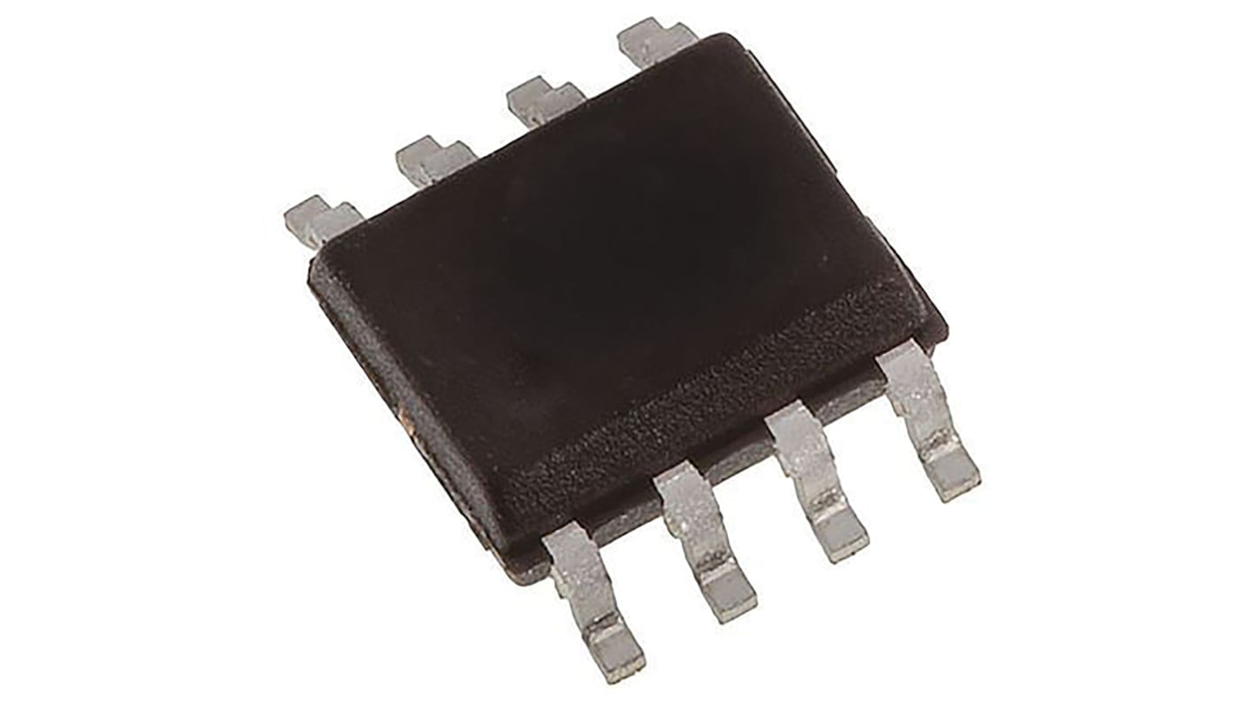
Infineon NOR 256 MB SPI Flash Memory 8-Pin SOIC, S25FL256LAGNFI010
- N° de stock RS:
- 184-0080
- Référence fabricant:
- S25FL256LAGNFI010
- Fabricant:
- Infineon

Sous-total (1 paquet de 2 unités)*
6,62 €
(TVA exclue)
8,02 €
(TVA incluse)
Frais de livraison offerts pour toute commande de plus de 90,00 €
En stock
- Plus 1 066 unité(s) expédiée(s) à partir du 13 juillet 2026
Besoin de plus? Cliquez sur " Vérifier les dates de livraison " pour plus de détails
Unité | Prix par unité | le paquet* |
|---|---|---|
| 2 + | 3,31 € | 6,62 € |
*Prix donné à titre indicatif
- N° de stock RS:
- 184-0080
- Référence fabricant:
- S25FL256LAGNFI010
- Fabricant:
- Infineon
Spécifications
Documentation technique
Législations et de normes
Détails du produit
Recherchez des produits similaires en sélectionnant un ou plusieurs attributs.
Sélectionner tout | Attribut | Valeur |
|---|---|---|
| Marque | Infineon | |
| Memory Size | 256MB | |
| Product Type | Flash Memory | |
| Interface Type | SPI | |
| Package Type | SOIC | |
| Pin Count | 8 | |
| Organisation | 32M x 8 bit | |
| Maximum Clock Frequency | 133MHz | |
| Mount Type | Surface | |
| Cell Type | NOR | |
| Minimum Supply Voltage | 2.7V | |
| Maximum Supply Voltage | 3.6V | |
| Timing Type | Synchronous | |
| Minimum Operating Temperature | -40°C | |
| Maximum Operating Temperature | 85°C | |
| Standards/Approvals | No | |
| Width | 5.28mm | |
| Height | 1.9mm | |
| Length | 5.28mm | |
| Series | S25FL256L | |
| Maximum Random Access Time | 8ns | |
| Number of Bits per Word | 8 | |
| Number of Words | 32M | |
| Automotive Standard | AEC-Q100 | |
| Sélectionner tout | ||
|---|---|---|
Marque Infineon | ||
Memory Size 256MB | ||
Product Type Flash Memory | ||
Interface Type SPI | ||
Package Type SOIC | ||
Pin Count 8 | ||
Organisation 32M x 8 bit | ||
Maximum Clock Frequency 133MHz | ||
Mount Type Surface | ||
Cell Type NOR | ||
Minimum Supply Voltage 2.7V | ||
Maximum Supply Voltage 3.6V | ||
Timing Type Synchronous | ||
Minimum Operating Temperature -40°C | ||
Maximum Operating Temperature 85°C | ||
Standards/Approvals No | ||
Width 5.28mm | ||
Height 1.9mm | ||
Length 5.28mm | ||
Series S25FL256L | ||
Maximum Random Access Time 8ns | ||
Number of Bits per Word 8 | ||
Number of Words 32M | ||
Automotive Standard AEC-Q100 | ||
The Cypress FL-L Family devices are Flash non-volatile memory products using: Floating Gate technology 65 nm process lithography The FL-L family connects to a host system via a Serial Peripheral Interface (SPI). Traditional SPI single bit serial input and output(Single I/O or SIO) is supported as well as optional two bit (Dual I/O or DIO) and four bit wide Quad I/O (QIO) and Quad Peripheral Interface (QPI) commands. In addition, there are Double Data Rate (DDR) read commands for QIO and QPI that transfer address and read data on both edges of the clock. The architecture features a Page Programming Buffer that allows up to 256-bytes to be programmed in one operation and provides individual 4KB sector, 32KB half block, 64KB block, or entire chip erase. By using FL-L family devices at the higher clock rates supported, with Quad commands, the instruction read transfer rate can match or exceed traditional parallel interface, asynchronous, NOR Flash memories, while reducing signal count dramatically. The FL-L family products offer high densities coupled with the flexibility and fast performance required by a variety of mobile or embedded applications. Provides an ideal storage solution for systems with limited space, signal connections, and power. These memories offer flexibility and performance well beyond ordinary serial flash devices. They are ideal for code shadowing to RAM,executing code directly (XIP), and storing re-programmable data.
Liens connexes
- Infineon NOR 256 MB SPI Flash Memory 8-Pin SOIC
- Infineon NOR 256 MB SPI Flash Memory 16-Pin SOIC
- Infineon NOR 256 MB SPI Flash Memory 16-Pin SOIC, S25FL256SAGMFVR00
- Infineon NOR 256 MB SPI Flash Memory 16-Pin SOIC, S25FL256LAGMFI000
- Infineon NOR 256 MB SPI Flash Memory 16-Pin SOIC, S25FL256SAGBHBA00
- Infineon NOR 256 MB SPI Flash Memory 16-Pin SOIC, S25FL256SAGMFI001
- Infineon NOR 256 MB SPI Flash Memory 16-Pin SOIC, S25FL256SAGMFI000
- Infineon NOR 256 MB Quad-SPI Flash Memory 16-Pin SOIC, S25FL256LAGMFN000