Altera PL-BYTEBLASTER2N,
- N° de stock RS:
- 729-4261
- Référence fabricant:
- PL-BYTEBLASTER2N
- Fabricant:
- Altera

Sous-total (1 unité)*
163,44 €
(TVA exclue)
197,76 €
(TVA incluse)
Frais de livraison offerts pour toute commande de plus de 90,00 €
En stock
- Plus 2 unité(s) expédiée(s) à partir du 20 juillet 2026
- Plus 1 unité(s) expédiée(s) à partir du 20 août 2026
Besoin de plus? Cliquez sur " Vérifier les dates de livraison " pour plus de détails
Unité | Prix par unité |
|---|---|
| 1 + | 163,44 € |
*Prix donné à titre indicatif
- N° de stock RS:
- 729-4261
- Référence fabricant:
- PL-BYTEBLASTER2N
- Fabricant:
- Altera
Spécifications
Documentation technique
Législations et de normes
Détails du produit
Recherchez des produits similaires en sélectionnant un ou plusieurs attributs.
Sélectionner tout | Attribut | Valeur |
|---|---|---|
| Marque | Altera | |
| Kit Contents | Ribbon Cable | |
| Kit Type | ByteBlaster II Parallel Port | |
| Standards/Approvals | No | |
| Sub Type | Programmer | |
| Product Type | Programmers & In-Circuit Emulator | |
| For Use With | Altera Device | |
| Sélectionner tout | ||
|---|---|---|
Marque Altera | ||
Kit Contents Ribbon Cable | ||
Kit Type ByteBlaster II Parallel Port | ||
Standards/Approvals No | ||
Sub Type Programmer | ||
Product Type Programmers & In-Circuit Emulator | ||
For Use With Altera Device | ||
- Pays d'origine :
- TW
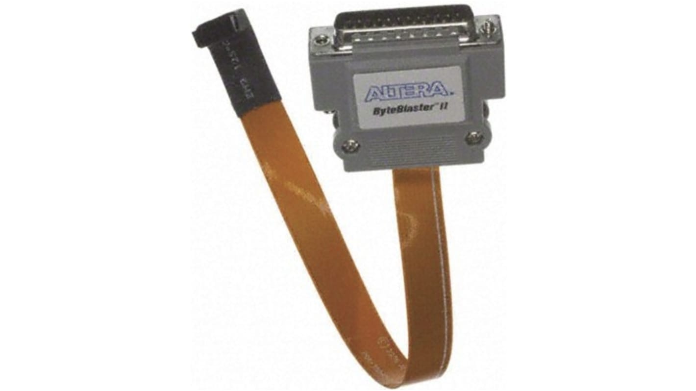
ByteBlaster II Programming Cable
The ByteBlaster™ II download cable allows you to program and configure Altera devices. This cable drives configuration data from a standard parallel printer port on a PC to the device on the PCB. Because design changes are downloaded directly to the device, prototyping is easy and you can accomplish multiple design iterations in quick succession.
Stratix® series FPGAs
Cyclone® series FPGAs
MAX® series CPLDs
Arria™ GX series FPGAs
APEX™ series FPGAs
ACEX® 1K FPGAs
Mercury™ FPGAs
FLEX 10K® series FPGAs
Excalibur™ FPGAs
EPC2, EPC4, EPC8 and EPC16 devices
EPCS1, EPCS4, EPCS16, EPCS64 and EPCS128 devices
An FPGA is a semiconductor device consisting of a matrix of Configurable Logic Blocks (CLBs) connected through programmable interconnects. The user determines these interconnections by programming SRAM. A CLB can be simple (AND, OR gates, etc) or complex (a block of RAM). The FPGA allows changes to be made to a design even after the device is soldered into a PCB.
Liens connexes
- Altera PL-USB-BLASTER-RCN,
- Altera FPGAs
- Altera CPLDs
- Altera EPC8QI100N, Configuration Memory 100-Pin PQFP
- Altera EPCS1SI8N, Configuration Memory 20MHz 8-Pin SOIC
- Altera EPCS16SI8N, Configuration Memory 20MHz 8-Pin SOIC
- Altera EPCS64SI16N, Configuration Memory 20MHz 16-Pin SOIC
- Altera EPCS4SI8N, Configuration Memory 20MHz 8-Pin SOIC