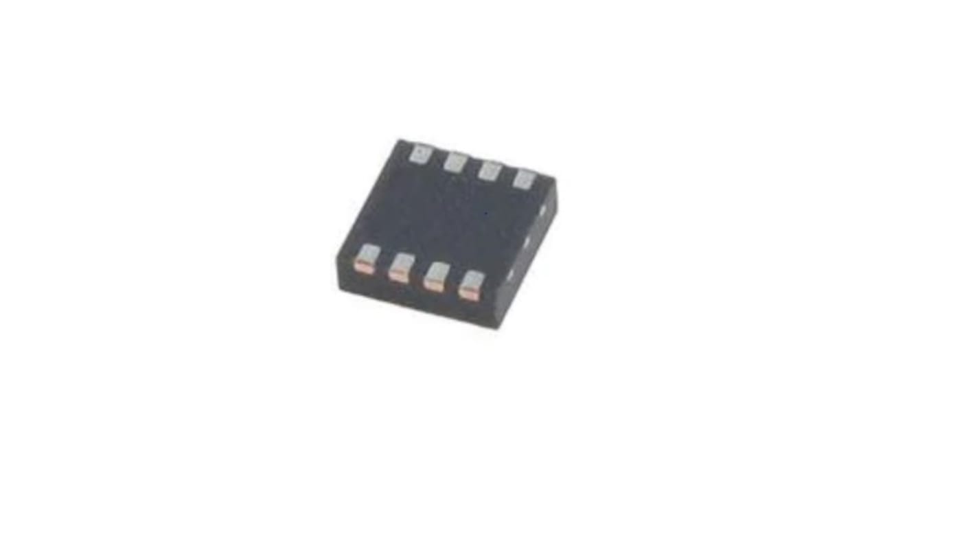
Renesas Electronics 5PB1102CMGI8 Clock Buffer, 8-Pin TSSOP
- N° de stock RS:
- 216-6164
- Référence fabricant:
- 5PB1102CMGI8
- Fabricant:
- Renesas Electronics

Sous-total (1 bobine de 4000 unités)*
3 704,00 €
(TVA exclue)
4 480,00 €
(TVA incluse)
Frais de livraison offerts pour toute commande de plus de 90,00 €
En stock
- Plus 4 000 unité(s) expédiée(s) à partir du 20 juillet 2026
Besoin de plus? Cliquez sur " Vérifier les dates de livraison " pour plus de détails
Unité | Prix par unité | la bobine* |
|---|---|---|
| 4000 + | 0,926 € | 3 704,00 € |
*Prix donné à titre indicatif
- N° de stock RS:
- 216-6164
- Référence fabricant:
- 5PB1102CMGI8
- Fabricant:
- Renesas Electronics
Spécifications
Documentation technique
Législations et de normes
Détails du produit
Recherchez des produits similaires en sélectionnant un ou plusieurs attributs.
Sélectionner tout | Attribut | Valeur |
|---|---|---|
| Marque | Renesas Electronics | |
| Product Type | Clock Buffer | |
| Mount Type | Surface | |
| Package Type | TSSOP | |
| Pin Count | 8 | |
| Minimum Supply Voltage | 1.8V | |
| Maximum Supply Voltage | 3.3V | |
| Minimum Operating Temperature | -40°C | |
| Maximum Operating Temperature | 85°C | |
| Length | 2mm | |
| Series | 5PB1102 | |
| Standards/Approvals | No | |
| Height | 0.5mm | |
| Automotive Standard | AEC-Q100 | |
| Sélectionner tout | ||
|---|---|---|
Marque Renesas Electronics | ||
Product Type Clock Buffer | ||
Mount Type Surface | ||
Package Type TSSOP | ||
Pin Count 8 | ||
Minimum Supply Voltage 1.8V | ||
Maximum Supply Voltage 3.3V | ||
Minimum Operating Temperature -40°C | ||
Maximum Operating Temperature 85°C | ||
Length 2mm | ||
Series 5PB1102 | ||
Standards/Approvals No | ||
Height 0.5mm | ||
Automotive Standard AEC-Q100 | ||
The Renesas Electronics 5PB11xx is a high-performance LVCMOS clock buffer family of devices. It has an additive phase jitter of 50fs RMS. There are five different fan-out variations available: 1:2 to 1:10. The 5PB11xx supports a synchronous glitch-free output enable (OE) function to eliminate any potential intermediate incorrect output clock cycles when enabling or disabling outputs. It can operate from a 1.8V to 3.3V supply.
High-performance 1:2, 1:4, 1:6, 1:8, 1:10 LVCMOS clock buffer
Very low pin-to-pin skew: < 50ps
Very low additive jitter: < 50fs
Supply voltage: 1.8V to 3.3V
3.3V tolerant input clock
fMAX = 200MHz
Integrated serial termination for 50Ω channel
Liens connexes
- Renesas Electronics 5PB1102CMGI8 Clock Buffer, 8-Pin TSSOP
- Renesas Electronics 5PB1104PGGI Clock Buffer, 8-Pin 4 TSSOP
- Renesas Electronics Clock Buffer 8-Pin TSSOP
- Renesas Electronics 5PB1104PGGK Clock Buffer 8-Pin TSSOP
- Renesas Electronics 5PB1104PGGI8 Clock Buffer 8-Pin TSSOP
- Renesas Electronics 5PB1102PGGK Clock Buffer 8-Pin TSSOP
- Renesas Electronics 2305-1DCGI8 Clock Buffer 8-Pin TSSOP
- Renesas Electronics 8305AGLF Clock Buffer, 16-Pin 4 TSSOP