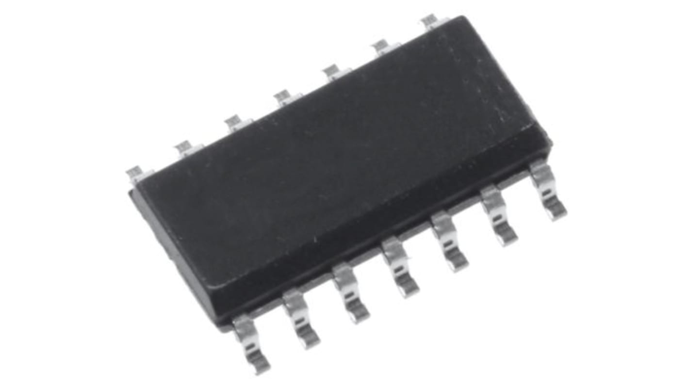
onsemi, Voltage Level Shifter Buffer 1 Buffer, 14-Pin SOIC
- N° de stock RS:
- 186-7319
- Référence fabricant:
- MM74HC125M
- Fabricant:
- onsemi

Offre groupée disponible
Consulter les options de prix de grosSous-total (1 tube de 55 unités)*
20,57 €
(TVA exclue)
24,915 €
(TVA incluse)
Frais de livraison offerts pour toute commande de plus de 90,00 €
En stock
- Plus 110 unité(s) expédiée(s) à partir du 27 juillet 2026
Besoin de plus? Cliquez sur " Vérifier les dates de livraison " pour plus de détails
Unité | Prix par unité | le tube* |
|---|---|---|
| 55 - 495 | 0,374 € | 20,57 € |
| 550 - 2695 | 0,29 € | 15,95 € |
| 2750 - 4070 | 0,283 € | 15,57 € |
| 4125 - 8195 | 0,275 € | 15,13 € |
| 8250 + | 0,269 € | 14,80 € |
*Prix donné à titre indicatif
- N° de stock RS:
- 186-7319
- Référence fabricant:
- MM74HC125M
- Fabricant:
- onsemi
Spécifications
Documentation technique
Législations et de normes
Détails du produit
Recherchez des produits similaires en sélectionnant un ou plusieurs attributs.
Sélectionner tout | Attribut | Valeur |
|---|---|---|
| Marque | onsemi | |
| Direction Type | Uni-Directional | |
| Product Type | Voltage Level Shifter | |
| Logic Family | HC | |
| Maximum Propagation Delay Time @ CL | 18ns | |
| Mount Type | Surface | |
| Package Type | SOIC | |
| Number of Elements per Chip | 1 | |
| Output Type | 3 State | |
| Pin Count | 14 | |
| Logic Function | Buffer | |
| Maximum Low Level Output Current | 7.8mA | |
| Maximum High Level Output Current | 7.8mA | |
| Minimum Supply Voltage | 2V | |
| Maximum Supply Voltage | 6V | |
| Translation | Buffer | |
| Minimum Operating Temperature | -40°C | |
| Maximum Operating Temperature | 85°C | |
| Height | 1.5mm | |
| Standards/Approvals | No | |
| Length | 8.75mm | |
| Series | MM74HC125 | |
| Automotive Standard | No | |
| Sélectionner tout | ||
|---|---|---|
Marque onsemi | ||
Direction Type Uni-Directional | ||
Product Type Voltage Level Shifter | ||
Logic Family HC | ||
Maximum Propagation Delay Time @ CL 18ns | ||
Mount Type Surface | ||
Package Type SOIC | ||
Number of Elements per Chip 1 | ||
Output Type 3 State | ||
Pin Count 14 | ||
Logic Function Buffer | ||
Maximum Low Level Output Current 7.8mA | ||
Maximum High Level Output Current 7.8mA | ||
Minimum Supply Voltage 2V | ||
Maximum Supply Voltage 6V | ||
Translation Buffer | ||
Minimum Operating Temperature -40°C | ||
Maximum Operating Temperature 85°C | ||
Height 1.5mm | ||
Standards/Approvals No | ||
Length 8.75mm | ||
Series MM74HC125 | ||
Automotive Standard No | ||
The MM74HC125 and MM74HC126 are general purpose 3-STATE high speed non-inverting buffers utilizing advanced silicon-gate CMOS technology. They have high drive current outputs which enable high speed operation even when driving large bus capacitances. These circuits possess the low power dissipation of CMOS circuitry, yet have speeds comparable to low power Schottky TTL circuits. Both circuits are capable of driving up to 15 low power Schottky inputs. The MM74HC125 require the 3-STATE control input C to be taken high to put the output into the high impedance condition, whereas the MM74HC126 require the control input to be low to put the output into high impedance. All inputs are protected from damage due to static discharge by diodes to VCC and ground.
Typical propagation delay: 13 ns
Wide operating voltage range: 2-6V
Low input current: 1 μA maximum
Low quiescent current: 80 μA maximum (74HC)
Fanout of 15 LS-TTL loads
Applications
This product is general usage and suitable for many different applications.