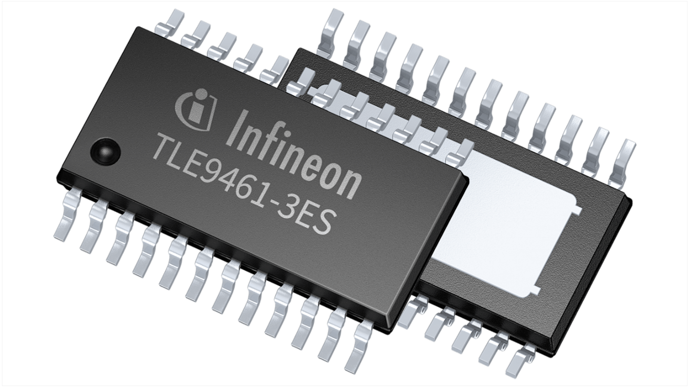
Infineon System-On-Chip 24-Pin TSDSO-24
- N° de stock RS:
- 244-2897
- Référence fabricant:
- TLE94613ESXUMA1
- Fabricant:
- Infineon

Sous-total (1 bobine de 3000 unités)*
4 284,00 €
(TVA exclue)
5 184,00 €
(TVA incluse)
Frais de livraison offerts pour toute commande de plus de 90,00 €
Temporairement en rupture de stock
- Expédition à partir du 01 avril 2027
Besoin de plus? Cliquez sur " Vérifier les dates de livraison " pour plus de détails
Unité | Prix par unité | la bobine* |
|---|---|---|
| 3000 + | 1,428 € | 4 284,00 € |
*Prix donné à titre indicatif
- N° de stock RS:
- 244-2897
- Référence fabricant:
- TLE94613ESXUMA1
- Fabricant:
- Infineon
Spécifications
Documentation technique
Législations et de normes
Détails du produit
Recherchez des produits similaires en sélectionnant un ou plusieurs attributs.
Sélectionner tout | Attribut | Valeur |
|---|---|---|
| Marque | Infineon | |
| Product Type | System-On-Chip | |
| Mount Type | Surface | |
| Package Type | TSDSO-24 | |
| Pin Count | 24 | |
| Interface Type | LIN, CAN | |
| Minimum Supply Voltage | -0.3V | |
| Maximum Supply Voltage | 28V | |
| Minimum Operating Temperature | -55°C | |
| Maximum Operating Temperature | 150°C | |
| Standards/Approvals | ISO 11898-2:2016, RoHS | |
| Height | 3.9mm | |
| Series | TLE9461-3ES | |
| Length | 8.65mm | |
| Automotive Standard | AEC-Q101, AEC-Q100 | |
| Sélectionner tout | ||
|---|---|---|
Marque Infineon | ||
Product Type System-On-Chip | ||
Mount Type Surface | ||
Package Type TSDSO-24 | ||
Pin Count 24 | ||
Interface Type LIN, CAN | ||
Minimum Supply Voltage -0.3V | ||
Maximum Supply Voltage 28V | ||
Minimum Operating Temperature -55°C | ||
Maximum Operating Temperature 150°C | ||
Standards/Approvals ISO 11898-2:2016, RoHS | ||
Height 3.9mm | ||
Series TLE9461-3ES | ||
Length 8.65mm | ||
Automotive Standard AEC-Q101, AEC-Q100 | ||
The Infineon TLE94613ESXUMA1 device is designed for various CAN automotive applications as main supply for the microcontroller and as interface for a CAN bus network including the CAN Partial Networking feature. To support these applications, the System Basis Chip (SBC) provides the main functions, such as a 5 V lowdropout voltage regulator (LDO) for e.g. a microcontroller supply, another 5 V low-dropout voltage regulator with off-board protection for e.g. sensor supply, a HS-CAN transceiver supporting CAN FD and CAN Partial Networking (incl. FD tolerant mode) for data transmission, a high-voltage GPIO with embedded protective functions and a 16-bit Serial Peripheral Interface (SPI) to control and monitor the device.
Fully compliant to “Hardware Requirements for LIN, CAN and FlexRay Interfaces in Automotive Applications” Revision 1.3, 2012-05-04
Charge pump-Output for N-channel MOSFET reverse-polarity protection with integrated spread spectrum modulation feature for optimum EMC performance
Universal High-Voltage Wake Input for voltage level monitoring and wake detection
General Purpose High-Voltage In- and Output (GPIO) configurable as Fail Output, Wake Input, Low-Side switch or High-Side switch
HIgh-Voltage Measurement Function as alternate pin assignment
Fail Outputs for Fail-Safe signalization
Configurable wake-up sources
Reset Output & Interrupt Output
Liens connexes
- Infineon TLE94613ESXUMA1 System-On-Chip 24-Pin TSDSO-24
- Infineon System-On-Chip 24-Pin TSDSO-24
- Infineon TLE94713ESXUMA1 System-On-Chip 24-Pin TSDSO-24
- Infineon TLE9471ESXUMA1 System-On-Chip 24-Pin TSDSO-24
- Infineon Power Switch IC 24-Pin, PG-TSDSO-24
- Infineon TLE75602ESHXUMA1 Power Switch IC 24-Pin, PG-TSDSO-24
- Infineon 24-Pin TSDSO
- Infineon 24-Pin TSDSO