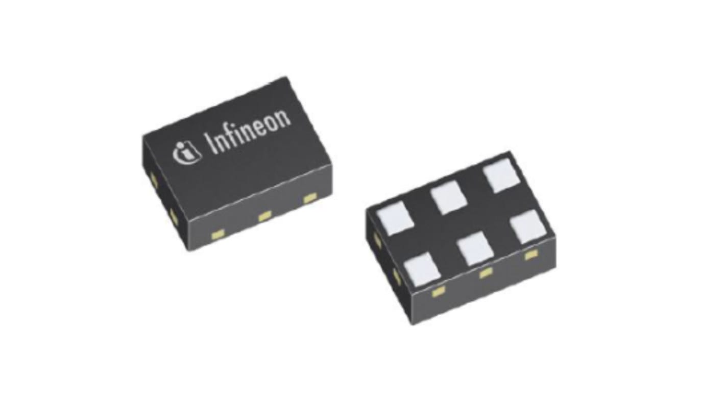
Infineon BGC100GN6E6327XTSA1 RF Switch, 6-Pin TSNP-6-2
- N° de stock RS:
- 273-5229
- Référence fabricant:
- BGC100GN6E6327XTSA1
- Fabricant:
- Infineon

Sous-total (1 bobine de 15000 unités)*
2 550,00 €
(TVA exclue)
3 150,00 €
(TVA incluse)
Informations sur le stock actuellement non accessibles - Veuillez vérifier plus tard
Unité | Prix par unité | la bobine* |
|---|---|---|
| 15000 + | 0,17 € | 2 550,00 € |
*Prix donné à titre indicatif
- N° de stock RS:
- 273-5229
- Référence fabricant:
- BGC100GN6E6327XTSA1
- Fabricant:
- Infineon
Spécifications
Documentation technique
Législations et de normes
Détails du produit
Recherchez des produits similaires en sélectionnant un ou plusieurs attributs.
Sélectionner tout | Attribut | Valeur |
|---|---|---|
| Marque | Infineon | |
| Technology | RF CMOS | |
| Product Type | RF Switch | |
| Sub Type | RF Switch | |
| Package Type | TSNP-6-2 | |
| Pin Count | 6 | |
| Mount Type | Surface | |
| Interface Type | GPIO | |
| Operating Band 1 Frequency | 0.6GHz | |
| Minimum Supply Voltage | 1.6V | |
| Operating Band 2 Frequency | 2.7GHz | |
| Maximum Supply Voltage | 3.4V | |
| Minimum Operating Temperature | -40°C | |
| Maximum Operating Temperature | 85°C | |
| Standards/Approvals | RoHS and WEEE | |
| Series | BGC100GN6 | |
| Height | 0.4mm | |
| Length | 1.1mm | |
| Automotive Standard | No | |
| Sélectionner tout | ||
|---|---|---|
Marque Infineon | ||
Technology RF CMOS | ||
Product Type RF Switch | ||
Sub Type RF Switch | ||
Package Type TSNP-6-2 | ||
Pin Count 6 | ||
Mount Type Surface | ||
Interface Type GPIO | ||
Operating Band 1 Frequency 0.6GHz | ||
Minimum Supply Voltage 1.6V | ||
Operating Band 2 Frequency 2.7GHz | ||
Maximum Supply Voltage 3.4V | ||
Minimum Operating Temperature -40°C | ||
Maximum Operating Temperature 85°C | ||
Standards/Approvals RoHS and WEEE | ||
Series BGC100GN6 | ||
Height 0.4mm | ||
Length 1.1mm | ||
Automotive Standard No | ||
- Pays d'origine :
- MY
The Infineon Bi directional coupler IC is designed for 2G, 3G, 4G RF front end applications. The device contains a bidirectional coupler operating in one or multiple bands within 0.6 GHz to 2.7 GHz frequency range. The coupled output contains a low pass filter for 5 GHz ISM blockers suppression. The coupler offers low insertion loss and high directivity. The coupler is controlled via a GPIO pin. No external power supply blocking or RF decoupling capacitors are required. The coupler is a fully integrated device deploying Infineon high volume RF CMOS technology. The device has a very small size of only 1.1 x 0.7 mm2 and a maximum height of 0.4 mm.
GPIO controlled
Integrated low pass filter
Supports all cellular standards
RoHS and WEEE compliant package
Fully integrated coupler in RF CMOS
Designed for low insertion loss and high directivity