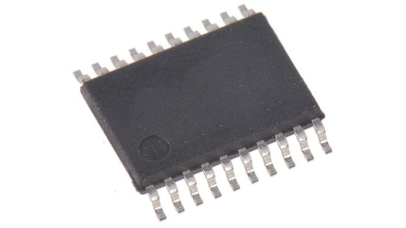
Renesas Electronics 9DB102BGILF, LVDS Buffer 2 TTL Buffer, 20-Pin TSSOP
- N° de stock RS:
- 217-7929
- Référence fabricant:
- 9DB102BGILF
- Fabricant:
- Renesas Electronics

Offre groupée disponible
Consulter les options de prix de grosSous-total (1 paquet de 5 unités)*
19,62 €
(TVA exclue)
23,74 €
(TVA incluse)
Frais de livraison offerts pour toute commande de plus de 90,00 €
En stock
- Plus 45 unité(s) expédiée(s) à partir du 20 juillet 2026
Besoin de plus? Cliquez sur " Vérifier les dates de livraison " pour plus de détails
Unité | Prix par unité | le paquet* |
|---|---|---|
| 5 - 5 | 3,924 € | 19,62 € |
| 10 - 20 | 3,54 € | 17,70 € |
| 25 - 95 | 3,332 € | 16,66 € |
| 100 - 245 | 2,902 € | 14,51 € |
| 250 + | 2,748 € | 13,74 € |
*Prix donné à titre indicatif
- N° de stock RS:
- 217-7929
- Référence fabricant:
- 9DB102BGILF
- Fabricant:
- Renesas Electronics
Spécifications
Documentation technique
Législations et de normes
Détails du produit
Recherchez des produits similaires en sélectionnant un ou plusieurs attributs.
Sélectionner tout | Attribut | Valeur |
|---|---|---|
| Marque | Renesas Electronics | |
| Number of Drivers | 2 | |
| Product Type | LVDS Buffer | |
| Input Type | TTL | |
| Sub Type | Buffer | |
| Output Type | Buffer | |
| Number of Elements per Chip | 2 | |
| Mount Type | Surface | |
| Package Type | TSSOP | |
| Pin Count | 20 | |
| Minimum Supply Voltage | 3V | |
| Maximum Supply Voltage | 3.3V | |
| Minimum Operating Temperature | -40°C | |
| ESD Protection | Yes | |
| Maximum Operating Temperature | 85°C | |
| Height | 1.05mm | |
| Length | 6.6mm | |
| Standards/Approvals | No | |
| Series | 9DB102 | |
| Automotive Standard | No | |
| Sélectionner tout | ||
|---|---|---|
Marque Renesas Electronics | ||
Number of Drivers 2 | ||
Product Type LVDS Buffer | ||
Input Type TTL | ||
Sub Type Buffer | ||
Output Type Buffer | ||
Number of Elements per Chip 2 | ||
Mount Type Surface | ||
Package Type TSSOP | ||
Pin Count 20 | ||
Minimum Supply Voltage 3V | ||
Maximum Supply Voltage 3.3V | ||
Minimum Operating Temperature -40°C | ||
ESD Protection Yes | ||
Maximum Operating Temperature 85°C | ||
Height 1.05mm | ||
Length 6.6mm | ||
Standards/Approvals No | ||
Series 9DB102 | ||
Automotive Standard No | ||
The Renesas Electronics 9DB102 zero-delay buffer supports PCI Express clocking requirements. The 9DB102 is driven by a differential SRC output pair from an IDT CK409/CK410-compliant main clock generator such as the 952601 or 954101. It attenuates jitter on the input clock and has a selectable PLL Band Width to maximize performance in systems with or without Spread- Spectrum clocking.
2 - 0.7 V HCSL differential output pairs
Phase jitter: PCIe Gen2 < 3.1 ps rms
Phase jitter: PCIe Gen1 < 86 ps peak to peak
Supports zero delay buffer mode and fanout mode
Bandwidth programming available
33-110 MHz operation in PLL mode
10-110 MHz operation in Bypass mode
Liens connexes
- Renesas Electronics 9DB102BGILF 20-Pin TSSOP
- Renesas Electronics 20-Pin TSSOP
- Renesas Electronics 9DB403DGILFT 20-Pin TSSOP
- Renesas Electronics Line Transceiver 20-Pin TSSOP
- Renesas Electronics ICL3222EIVZ-T Line Transceiver 20-Pin TSSOP
- Renesas Electronics ICL3223EIVZ 20-Channel Line Transceiver 20-Pin TSSOP
- Renesas Electronics 853S014AGILF Buffer 20-Pin TSSOP
- Texas Instruments SN65LVDS84AQDGG 48-Pin TSSOP