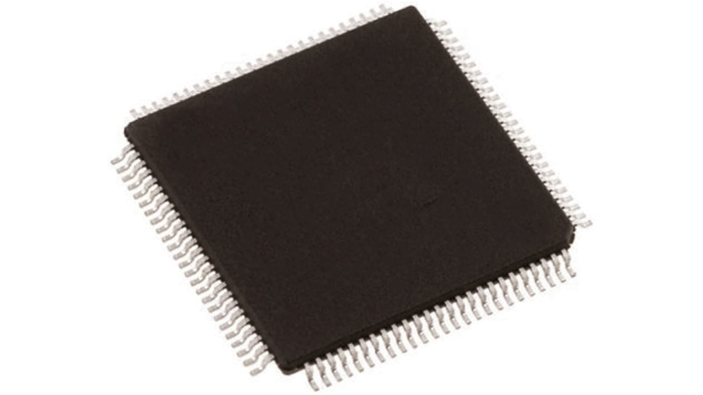
Lattice FPGA iCE40HX1K-VQ100 iCE40 1280 Cells, 64000 bit 160 Blocks, 100-Pin VQFP
- N° de stock RS:
- 772-0045
- Référence fabricant:
- iCE40HX1K-VQ100
- Fabricant:
- Lattice Semiconductor

Offre groupée disponible
Consulter les options de prix de grosSous-total (1 unité)*
6,44 €
(TVA exclue)
7,79 €
(TVA incluse)
Frais de livraison offerts pour toute commande de plus de 90,00 €
Temporairement en rupture de stock
- 76 unité(s) expédiée(s) à partir du 16 juillet 2026
Besoin de plus? Cliquez sur " Vérifier les dates de livraison " pour plus de détails
Unité | Prix par unité |
|---|---|
| 1 - 9 | 6,44 € |
| 10 - 49 | 6,28 € |
| 50 - 99 | 6,11 € |
| 100 - 199 | 5,96 € |
| 200 + | 5,81 € |
*Prix donné à titre indicatif
- N° de stock RS:
- 772-0045
- Référence fabricant:
- iCE40HX1K-VQ100
- Fabricant:
- Lattice Semiconductor
Spécifications
Documentation technique
Législations et de normes
Détails du produit
Recherchez des produits similaires en sélectionnant un ou plusieurs attributs.
Sélectionner tout | Attribut | Valeur |
|---|---|---|
| Marque | Lattice Semiconductor | |
| Series | iCE40 | |
| Product Type | FPGA | |
| Number of Logic Cells | 1280 | |
| Number of Logic Units | 160 | |
| Number of Registers | 1280 | |
| Mount Type | Surface | |
| Package Type | VQFP | |
| Minimum Supply Voltage | 1.14V | |
| Pin Count | 100 | |
| Maximum Supply Voltage | 1.26V | |
| Number of RAM Bits | 64000bit | |
| Minimum Operating Temperature | -40°C | |
| Maximum Operating Temperature | 85°C | |
| Standards/Approvals | No | |
| Height | 1.05mm | |
| Length | 14mm | |
| Automotive Standard | No | |
| Sélectionner tout | ||
|---|---|---|
Marque Lattice Semiconductor | ||
Series iCE40 | ||
Product Type FPGA | ||
Number of Logic Cells 1280 | ||
Number of Logic Units 160 | ||
Number of Registers 1280 | ||
Mount Type Surface | ||
Package Type VQFP | ||
Minimum Supply Voltage 1.14V | ||
Pin Count 100 | ||
Maximum Supply Voltage 1.26V | ||
Number of RAM Bits 64000bit | ||
Minimum Operating Temperature -40°C | ||
Maximum Operating Temperature 85°C | ||
Standards/Approvals No | ||
Height 1.05mm | ||
Length 14mm | ||
Automotive Standard No | ||
Field Programmable Gate Arrays, Lattice Semiconductor
An FPGA is a semiconductor device consisting of a Matrix of Configurable Logic Blocks (CLBs) connected through programmable interconnects. The user determines these interconnections by programming SRAM. A CLB can be simple (AND, OR gates, etc) or complex (a Block of RAM). The FPGA allows changes to be MADE to a design even after the device is soldered into a PCB.
Liens connexes
- Lattice FPGA iCE40 1280 Cells 100-Pin VQFP
- Lattice FPGA iCE40 LP/HX 1280 Cells 49-Pin UCBGA
- Lattice FPGA iCE40LP1K-CM49 iCE40 LP/HX 1280 Cells 49-Pin UCBGA
- Lattice FPGA iCE40 3520 Cells 144-Pin TQFP
- Lattice FPGA iCE40HX4K-TQ144 iCE40 3520 Cells 144-Pin TQFP
- Microchip FPGA A3P250-VQG100I A3P250 6144 Cells 36 bit 6144 Blocks, 100-Pin VQFP
- SMC VVQ100, VVQ100-10A-2
- SICK UHF Transponder Transponder, 64000 bit