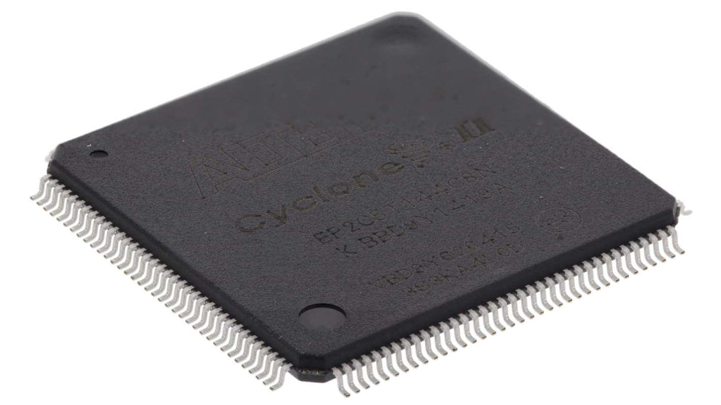
Altera FPGA EP2C5T144C8N Cyclone II 4608 Cells, 4608 Blocks, 144-Pin TQFP
- N° de stock RS:
- 169-5507
- Référence fabricant:
- EP2C5T144C8N
- Fabricant:
- Altera

Sous-total (1 plateau de 60 unités)*
1 941,90 €
(TVA exclue)
2 349,72 €
(TVA incluse)
Frais de livraison offerts pour toute commande de plus de 90,00 €
En stock
- 180 unité(s) prête(s) à être expédiée(s) d'un autre centre de distribution
Besoin de plus? Cliquez sur " Vérifier les dates de livraison " pour plus de détails
Unité | Prix par unité | le plateau* |
|---|---|---|
| 60 + | 32,365 € | 1 941,90 € |
*Prix donné à titre indicatif
- N° de stock RS:
- 169-5507
- Référence fabricant:
- EP2C5T144C8N
- Fabricant:
- Altera
Spécifications
Documentation technique
Législations et de normes
Détails du produit
Recherchez des produits similaires en sélectionnant un ou plusieurs attributs.
Sélectionner tout | Attribut | Valeur |
|---|---|---|
| Marque | Altera | |
| Series | Cyclone II | |
| Product Type | FPGA | |
| Number of Logic Cells | 4608 | |
| Number of Logic Units | 4608 | |
| Number of Multipliers | 13 | |
| Mount Type | Surface | |
| Minimum Supply Voltage | 1.15V | |
| Package Type | TQFP | |
| Maximum Supply Voltage | 1.25V | |
| Pin Count | 144 | |
| Minimum Operating Temperature | 0°C | |
| Maximum Operating Temperature | 85°C | |
| Height | 1.4mm | |
| Length | 20mm | |
| Standards/Approvals | No | |
| Automotive Standard | No | |
| Sélectionner tout | ||
|---|---|---|
Marque Altera | ||
Series Cyclone II | ||
Product Type FPGA | ||
Number of Logic Cells 4608 | ||
Number of Logic Units 4608 | ||
Number of Multipliers 13 | ||
Mount Type Surface | ||
Minimum Supply Voltage 1.15V | ||
Package Type TQFP | ||
Maximum Supply Voltage 1.25V | ||
Pin Count 144 | ||
Minimum Operating Temperature 0°C | ||
Maximum Operating Temperature 85°C | ||
Height 1.4mm | ||
Length 20mm | ||
Standards/Approvals No | ||
Automotive Standard No | ||
Cyclone FPGA, Altera
An FPGA is a semiconductor device consisting of a matrix of Configurable Logic Blocks (CLBs) connected through programmable interconnects. The user determines these interconnections by programming SRAM. A CLB can be simple (AND, OR gates, etc) or complex (a block of RAM). The FPGA allows changes to be made to a design even after the device is soldered into a PCB.
Liens connexes
- Altera FPGA Cyclone II 4608 Cells 144-Pin TQFP
- Altera FPGA EP2C5T144I8N Cyclone II 4608 Cells 144-Pin TQFP
- Altera FPGA Cyclone II 4608 Cells 208-Pin PQFP
- Altera FPGA EP2C5Q208C8N Cyclone II 4608 Cells 208-Pin PQFP
- Altera FPGA EP1C3T100C8N 59904bit 100-Pin TQFP
- Altera FPGA Cyclone IV 6272 Cells 144-Pin EQFP
- Altera FPGA Cyclone IV 15408 Cells 144-Pin EQFP
- Altera FPGA EP4CE15E22C8N Cyclone IV 15408 Cells 144-Pin EQFP