Digilent 410-292 Nexys A7-100T Nexys 4 DDR Artix-7 Development Board ADC1410 for DAC121S101
- N° de stock RS:
- 134-6465
- Numéro d'article Distrelec:
- 300-44-278
- Référence fabricant:
- 410-292 Nexys A7-100T
- Fabricant:
- Digilent

Offre groupée disponible
Consulter les options de prix de grosSous-total (1 unité)*
350,72 €
(TVA exclue)
424,37 €
(TVA incluse)
Frais de livraison offerts pour toute commande de plus de 90,00 €
En stock
- 4 unité(s) prête(s) à être expédiée(s) d'un autre centre de distribution
- Plus 22 unité(s) expédiée(s) à partir du 14 août 2026
- Plus 14 unité(s) expédiée(s) à partir du 04 septembre 2026
Besoin de plus? Cliquez sur " Vérifier les dates de livraison " pour plus de détails
Unité | Prix par unité |
|---|---|
| 1 - 1 | 350,72 € |
| 2 - 4 | 341,72 € |
| 5 + | 333,18 € |
*Prix donné à titre indicatif
- N° de stock RS:
- 134-6465
- Numéro d'article Distrelec:
- 300-44-278
- Référence fabricant:
- 410-292 Nexys A7-100T
- Fabricant:
- Digilent
Spécifications
Documentation technique
Législations et de normes
Détails du produit
Recherchez des produits similaires en sélectionnant un ou plusieurs attributs.
Sélectionner tout | Attribut | Valeur |
|---|---|---|
| Marque | Digilent | |
| Programmable Logic Technology | FPGA | |
| Product Type | Programmable Logic Development Kit | |
| Kit Classification | Development Board | |
| For Use With | DAC121S101 | |
| Featured Device | ADC1410 | |
| Kit Name | Nexys 4 DDR Artix-7 | |
| Standards/Approvals | RoHS | |
| Sélectionner tout | ||
|---|---|---|
Marque Digilent | ||
Programmable Logic Technology FPGA | ||
Product Type Programmable Logic Development Kit | ||
Kit Classification Development Board | ||
For Use With DAC121S101 | ||
Featured Device ADC1410 | ||
Kit Name Nexys 4 DDR Artix-7 | ||
Standards/Approvals RoHS | ||
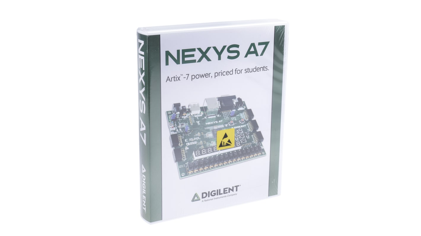
Nexys 4 DDR Artix-7 FPGA Trainer Board
The Nexys 4 is an FPGA development board designed for the educational market, featuring Xilinx Artix-7 architecture. The Nexys 4 DDR is compatible with the high-performance Vivado Design Suite as well as the ISE® toolset, which includes ChipScope™ and EDK. WebPACK editions of these toolsets can be downloaded for free from Xilinx. Expanded features are available through purchase of the Design Edition.
Xilinx Artix-7 FPGA (XC7A100T-1CSG324C) Features
• 101440 logic cells in 15850 slices (each slice contains 4 x 6-input LUTs and 8 x flip-flops);• 4860Kbit Fast Block RAM;• 6 x Clock Management Tiles, each with a phase-locked loop (PLL);• 240 x DSP slices;• Internal clock speeds exceeding 450MHz;• On-chip Analogue-to-Digital Converter (XADC)
Nexys 4 DDR Board Features
• MT47H64M16HR-25 128MiB DDR2 SDRAM
• S25FL128S 16MiB Quad-SPI Serial Flash memory
• ADXL362 SPI bus 3-axis accelerometer
• ADT7420 I²C bus temperature sensor
• ADMP421 MEMS microphone with PDM output
• Programmable over JTAG, Quad-SPI or USB
• FPGA Programming-Done LED
• 2 x 4-digit 7-segment LED displays
• 16 x User LEDs
• 2 x User RGB LEDs
• 5 x User Pushbuttons
• 16 x User Slide-Switches
• USB-UART Bridge via microUSB socket
• USB-A HID Host socket for mice, keyboards and memory sticks
• 12-bit VGA display output on DE15 connector
• RJ45 socket for 10/100 Ethernet connection
• 3.5mm jack socket for mono audio output
• microSD card slot
• 4 x Standard Pmod™ 2 x 6-pin connectors
• Analogue XADC Pmod™ 2 x 6-pin connector
• Powered from either USB, barrel jack socket or external battery pack
An FPGA is a semiconductor device consisting of a matrix of Configurable Logic Blocks (CLBs) connected through programmable interconnects. The user determines these interconnections by programming SRAM. A CLB can be simple (AND, OR gates, etc) or complex (a block of RAM). The FPGA allows changes to be made to a design even after the device is soldered into a PCB.
Supplied with
Hardshell plastic case with protective foam, USB cable
Liens connexes
- Digilent 410-316 Nexys Video Artix-7 Development Board ADC1410 for DAC121S101
- Digilent 410-328-35 Cmod A7 Artix-7 Module ADC1410 for DAC121S101
- Digilent 410-183 Basys Artix-7 Development Board ADC1410 for DAC121S101
- Digilent 410-300 GENESYS2 KINTEX-7 Development Board ADC1410 for DAC121S101
- Digilent 410-319-1 FPGA Development Board for Makers and Hobbyists Development Board ADC1410 for DAC121S101
- Digilent USB104 A7: Artix-7 FPGA Development Board in PC/104 Form Factor Xilinx Artix-7 XC7A100T Development Board for
- Digilent 410-428 Analogue Discovery Studio Logarithmic Amplifier Development Module for Nexys A7 for Analog Discovery
- Trenz Electronic GmbH TE0711-02-72C-1-A AMD Artix 7 Module AMD Artix 7A100T for Programmable Logic