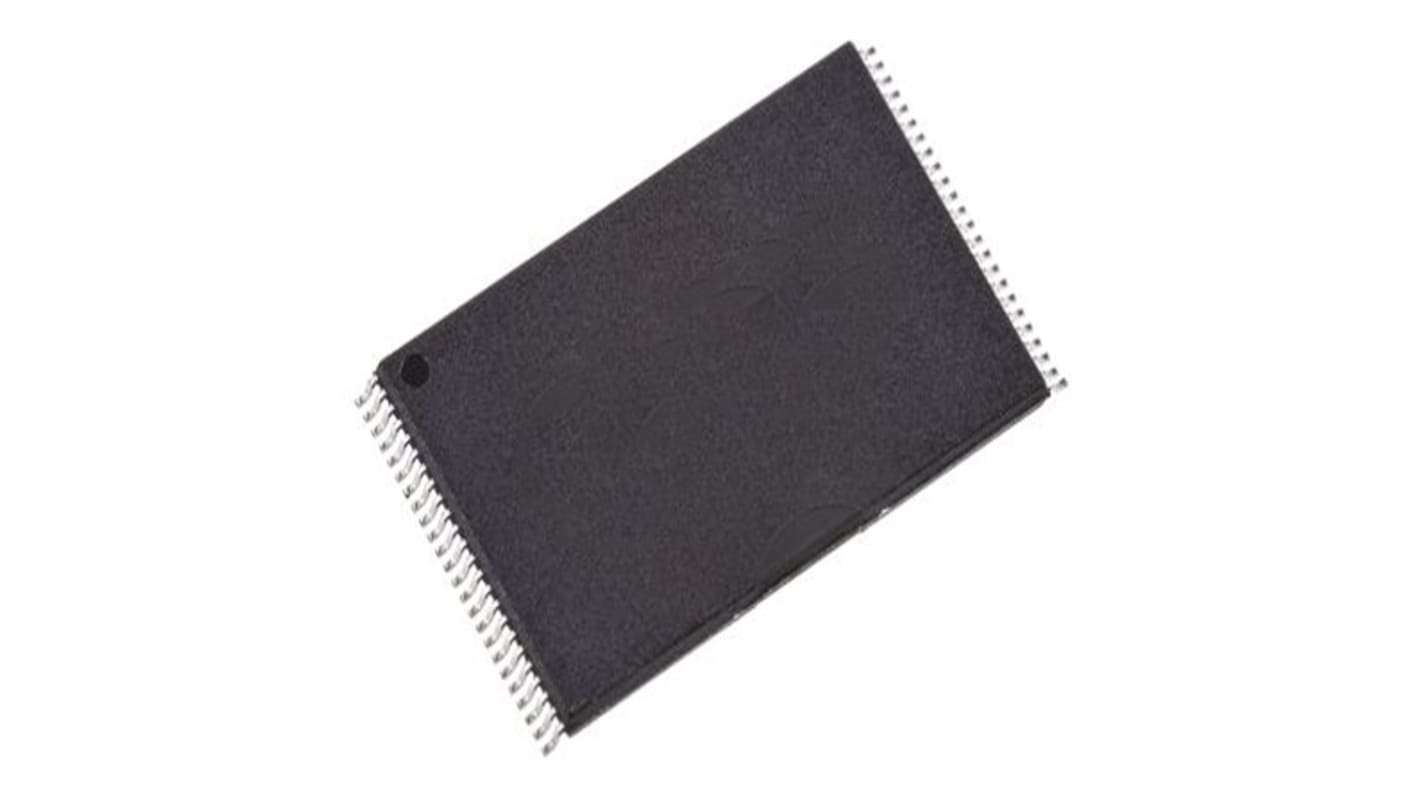
Infineon 32 MB SPI Flash Memory 48-Pin TSOP
- N° de stock RS:
- 273-7547
- Référence fabricant:
- S29JL032J70TFI310
- Fabricant:
- Infineon

Offre groupée disponible
Consulter les options de prix de grosSous-total (1 unité)*
4,93 €
(TVA exclue)
5,97 €
(TVA incluse)
Frais de livraison offerts pour toute commande de plus de 90,00 €
Dernier stock RS
- 601 dernière(s) unité(s), prête(s) à l'envoi d'un autre centre de distribution
Unité | Prix par unité |
|---|---|
| 1 - 9 | 4,93 € |
| 10 - 24 | 4,80 € |
| 25 - 49 | 4,67 € |
| 50 - 99 | 4,55 € |
| 100 + | 4,43 € |
*Prix donné à titre indicatif
- N° de stock RS:
- 273-7547
- Référence fabricant:
- S29JL032J70TFI310
- Fabricant:
- Infineon
Spécifications
Documentation technique
Législations et de normes
Détails du produit
Recherchez des produits similaires en sélectionnant un ou plusieurs attributs.
Sélectionner tout | Attribut | Valeur |
|---|---|---|
| Marque | Infineon | |
| Product Type | Flash Memory | |
| Memory Size | 32MB | |
| Interface Type | SPI | |
| Package Type | TSOP | |
| Pin Count | 48 | |
| Maximum Clock Frequency | 133MHz | |
| Minimum Supply Voltage | 2.7V | |
| Maximum Supply Voltage | 3.6V | |
| Minimum Operating Temperature | -40°C | |
| Maximum Operating Temperature | 85°C | |
| Standards/Approvals | RoHS | |
| Maximum Random Access Time | 15ns | |
| Automotive Standard | AEC-Q100 | |
| Sélectionner tout | ||
|---|---|---|
Marque Infineon | ||
Product Type Flash Memory | ||
Memory Size 32MB | ||
Interface Type SPI | ||
Package Type TSOP | ||
Pin Count 48 | ||
Maximum Clock Frequency 133MHz | ||
Minimum Supply Voltage 2.7V | ||
Maximum Supply Voltage 3.6V | ||
Minimum Operating Temperature -40°C | ||
Maximum Operating Temperature 85°C | ||
Standards/Approvals RoHS | ||
Maximum Random Access Time 15ns | ||
Automotive Standard AEC-Q100 | ||
The Infineon Flash Memory is a 32 Mb, 3.0 volt only flash memory device, organized as 2097152 words of 16 bits each or 4194304 bytes of 8 bits each. Word mode data appears on DQ15 to DQ0 and byte mode data appears on DQ7 to DQ0. The device is designed to be programmed in system with the standard 3.0 volt VCC supply and can also be programmed in standard EPROM programmers. The device is available with an access time of 60 or 70 ns. The device requires only a single 3.0 volt power supply for both read and write functions. Internally generated and regulated voltages are provided for the program and erase operations.
Hardware reset pin
20 years data retention
Compatible with JEDEC standards
Four bank architectures available
Unlock bypass program command
Simultaneous Read and Write operations
Zero latency between read and write operations
Liens connexes
- Infineon 32 MB SPI Flash Memory 48-Pin TSOP, S29JL032J70TFI310
- Infineon 32 MB SPI Flash Memory 48-Pin TSOP
- Infineon 32 MB SPI Flash Memory 48-Pin TSOP, S29JL032J70TFI320
- Infineon 32 MB SPI Flash Memory 48-Pin TSOP, S29JL032J70TFI210
- Infineon 64 MB SPI Flash Memory 48-Pin TSOP
- Infineon 64 MB SPI Flash Memory 48-Pin TSOP, S29GL064S70TFI060
- Infineon NOR 8 MB SPI Flash Memory 48-Pin TSOP
- Infineon NOR 8 MB SPI Flash Memory 48-Pin TSOP, S29AL008J55TFIR20