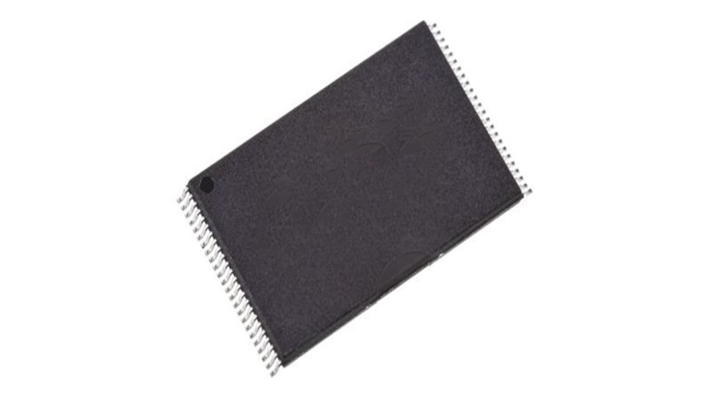
Infineon NOR 8 MB SPI Flash Memory 48-Pin TSOP, S29AL008J70TFI020
- N° de stock RS:
- 273-7518
- Référence fabricant:
- S29AL008J70TFI020
- Fabricant:
- Infineon

Offre groupée disponible
Consulter les options de prix de grosSous-total (1 plateau de 96 unités)*
224,64 €
(TVA exclue)
271,68 €
(TVA incluse)
Frais de livraison offerts pour toute commande de plus de 90,00 €
Dernier stock RS
- 480 dernière(s) unité(s), prête(s) à l'envoi d'un autre centre de distribution
Unité | Prix par unité | le plateau* |
|---|---|---|
| 96 - 96 | 2,34 € | 224,64 € |
| 192 + | 2,258 € | 216,77 € |
*Prix donné à titre indicatif
- N° de stock RS:
- 273-7518
- Référence fabricant:
- S29AL008J70TFI020
- Fabricant:
- Infineon
Spécifications
Documentation technique
Législations et de normes
Détails du produit
Recherchez des produits similaires en sélectionnant un ou plusieurs attributs.
Sélectionner tout | Attribut | Valeur |
|---|---|---|
| Marque | Infineon | |
| Memory Size | 8MB | |
| Product Type | Flash Memory | |
| Interface Type | SPI | |
| Package Type | TSOP | |
| Pin Count | 48 | |
| Maximum Clock Frequency | 133MHz | |
| Cell Type | NOR | |
| Maximum Supply Voltage | 3.6V | |
| Minimum Supply Voltage | 2.7V | |
| Minimum Operating Temperature | -40°C | |
| Maximum Operating Temperature | 125°C | |
| Standards/Approvals | No | |
| Supply Current | 20mA | |
| Automotive Standard | AEC-Q100 Grade 1, AEC-Q100 Grade 3 | |
| Series | S29AL008J | |
| Sélectionner tout | ||
|---|---|---|
Marque Infineon | ||
Memory Size 8MB | ||
Product Type Flash Memory | ||
Interface Type SPI | ||
Package Type TSOP | ||
Pin Count 48 | ||
Maximum Clock Frequency 133MHz | ||
Cell Type NOR | ||
Maximum Supply Voltage 3.6V | ||
Minimum Supply Voltage 2.7V | ||
Minimum Operating Temperature -40°C | ||
Maximum Operating Temperature 125°C | ||
Standards/Approvals No | ||
Supply Current 20mA | ||
Automotive Standard AEC-Q100 Grade 1, AEC-Q100 Grade 3 | ||
Series S29AL008J | ||
The Infineon Flash Memory requires only a single 3.0 volt power supply for both read and write functions. Internally generated and regulated voltages are provided for the program and erase operations. It offers access times of up to 55 ns allowing high speed microprocessors to operate without wait states. To eliminate bus contention the device has separate chip enable, write enable and output enable controls. This Flash memory offers two power saving features. When addresses have been stable for a specified amount of time, the device enters the automatic sleep mode. The system can also place the device into the standby mode. Power consumption is greatly reduced in both these modes.
Hardware reset pin
Secured silicon sector region
Single power supply operation
Minimum 20 year data retention
Unlock bypass program command
Superior inadvertent write protection
Liens connexes
- Infineon NOR 8 MB SPI Flash Memory 48-Pin TSOP
- Infineon NOR 8 MB SPI Flash Memory 48-Pin TSOP, S29AL008J55TFIR20
- Infineon NOR 16 MB SPI Flash Memory 48-Pin TSOP, S29AL016J70TFI020
- Infineon NOR 16 MB SPI Flash Memory 48-Pin TSOP, S29AL016J70TFI010
- Infineon NOR 8 MB SPI Flash Memory Device 48-Pin TSOP
- Infineon NOR 8 MB SPI Flash Memory Device 48-Pin TSOP, S29AL008J70BFI020
- Infineon NOR 32 MB CFI Flash Memory 48-Pin TSOP
- Infineon NOR 16 MB CFI Flash Memory 48-Pin TSOP