Nexperia, Decoder, 6-Pin TSSOP
- N° de stock RS:
- 152-3694P
- Référence fabricant:
- 74LVC1G19GW,125
- Fabricant:
- Nexperia

Sous-total 100 unités (conditionné en bande continue)*
4,30 €
(TVA exclue)
5,20 €
(TVA incluse)
Frais de livraison offerts pour toute commande de plus de 90,00 €
En stock
- 1 800 unité(s) prête(s) à être expédiée(s) d'un autre centre de distribution
Besoin de plus? Cliquez sur " Vérifier les dates de livraison " pour plus de détails
Unité | Prix par unité |
|---|---|
| 100 + | 0,043 € |
*Prix donné à titre indicatif
- N° de stock RS:
- 152-3694P
- Référence fabricant:
- 74LVC1G19GW,125
- Fabricant:
- Nexperia
Spécifications
Documentation technique
Législations et de normes
Détails du produit
Recherchez des produits similaires en sélectionnant un ou plusieurs attributs.
Sélectionner tout | Attribut | Valeur |
|---|---|---|
| Marque | Nexperia | |
| Product Type | Decoder | |
| Logic Family | 74LVC | |
| Number of Inputs | 2 | |
| Logic Function | Demultiplexer, Decoder | |
| Mount Type | Surface | |
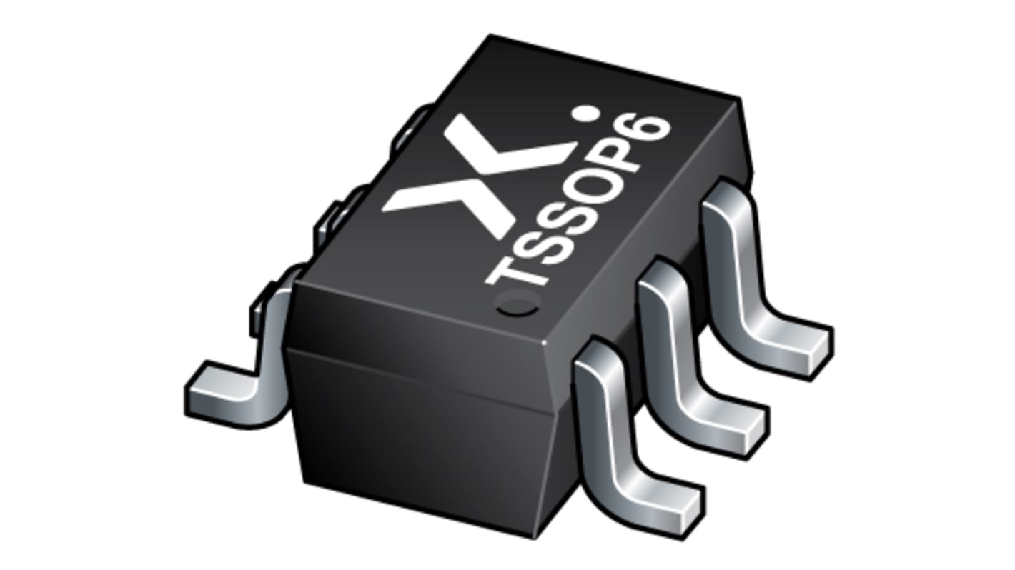
| Package Type | TSSOP | |
| Pin Count | 6 | |
| Minimum Supply Voltage | 1.65V | |
| Maximum Supply Voltage | 5.5V | |
| Minimum Operating Temperature | -40°C | |
| Maximum Operating Temperature | 125°C | |
| Height | 1mm | |
| Length | 2.2mm | |
| Standards/Approvals | No | |
| Series | 74LVC | |
| Automotive Standard | No | |
| Sélectionner tout | ||
|---|---|---|
Marque Nexperia | ||
Product Type Decoder | ||
Logic Family 74LVC | ||
Number of Inputs 2 | ||
Logic Function Demultiplexer, Decoder | ||
Mount Type Surface | ||
Package Type TSSOP | ||
Pin Count 6 | ||
Minimum Supply Voltage 1.65V | ||
Maximum Supply Voltage 5.5V | ||
Minimum Operating Temperature -40°C | ||
Maximum Operating Temperature 125°C | ||
Height 1mm | ||
Length 2.2mm | ||
Standards/Approvals No | ||
Series 74LVC | ||
Automotive Standard No | ||
The 74LVC1G19 is a 1-of-2 decoder/demultiplexer with a common output enable. This device buffers the data on input A and passes it to the outputs 1Y (true) and 2Y (complement) when the enable (E) input signal is LOW. Inputs can be driven from either 3.3 V or 5 V devices. These features allow the use of these devices in a mixed 3.3 V and 5 V environment. This device is fully specified for partial power-down applications using IOFF. The IOFF circuitry disables the output, preventing the damaging backflow current through the device when it is powered down.
Wide supply voltage range from 1.65 V to 5.5 V
5 V tolerant inputs for interfacing with 5 V logic
High noise immunity
CMOS low power consumption
Latch-up performance exceeds 250 mA
Direct Interface with TTL levels
Inputs accept voltages up to 5 V
Multiple package options