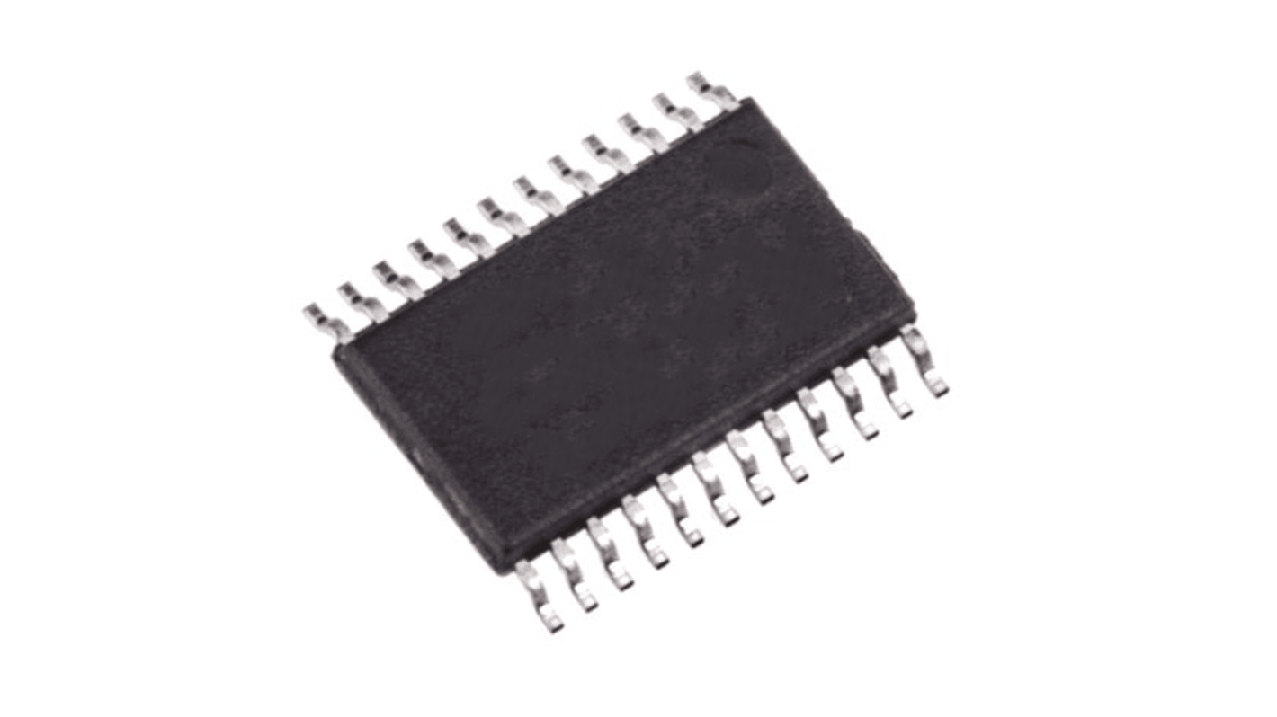
Renesas Electronics 5V2310PGGI High Performance Clock Buffer 24-Pin TSSOP
- N° de stock RS:
- 254-4947
- Référence fabricant:
- 5V2310PGGI
- Fabricant:
- Renesas Electronics

Actuellement indisponible
Nous ne savons pas si cet article sera de nouveau disponible. RS a l'intention de le retirer de son assortiment sous peu.
- N° de stock RS:
- 254-4947
- Référence fabricant:
- 5V2310PGGI
- Fabricant:
- Renesas Electronics
Spécifications
Documentation technique
Législations et de normes
Détails du produit
Recherchez des produits similaires en sélectionnant un ou plusieurs attributs.
Sélectionner tout | Attribut | Valeur |
|---|---|---|
| Marque | Renesas Electronics | |
| Product Type | High Performance Clock Buffer | |
| Maximum Input Frequency | 200MHz | |
| Maximum Propagation Delay Time | 2.8ns | |
| Mount Type | Surface | |
| Package Type | TSSOP | |
| Pin Count | 24 | |
| Number of Outputs | 10 | |
| Minimum Supply Voltage | 2.3V | |
| Maximum Supply Voltage | 3.6V | |
| Minimum Operating Temperature | -40°C | |
| Maximum Operating Temperature | 85°C | |
| Series | IDT5V2310 | |
| Standards/Approvals | RoHS | |
| Automotive Standard | No | |
| Sélectionner tout | ||
|---|---|---|
Marque Renesas Electronics | ||
Product Type High Performance Clock Buffer | ||
Maximum Input Frequency 200MHz | ||
Maximum Propagation Delay Time 2.8ns | ||
Mount Type Surface | ||
Package Type TSSOP | ||
Pin Count 24 | ||
Number of Outputs 10 | ||
Minimum Supply Voltage 2.3V | ||
Maximum Supply Voltage 3.6V | ||
Minimum Operating Temperature -40°C | ||
Maximum Operating Temperature 85°C | ||
Series IDT5V2310 | ||
Standards/Approvals RoHS | ||
Automotive Standard No | ||
The Renesas Electronics high performance, low skew clock buffer that operates up to 200MHz. Two banks of five outputs each provide low skew copies of CLK. Through the use of control pins 1G and 2G, the outputs of banks 1Y(0:4) and 2Y(0:4) can be placed in a low state regardless of CLK input. The device operates in 2.5V and 3.3V environments. The built-in output enable glitch suppression ensures a synchronized output enable sequence to distribute full period clock signals. The IDT5V2310 is characterized for operation from -40°C to +85°C.
High performance 1:10 clock driver for general purpose applications
Pin-to-pin skew < 100 ps
VDD range is 2.3 V to 3.6 V
Output enable glitch suppression
Distributes one clock input to two banks of five outputs
25 Ω on-chip series dampening resistors
Available in TSSOP package
Liens connexes
- Renesas Electronics High Performance Clock Buffer 24-Pin TSSOP
- Renesas Electronics Clock Buffer 28-Pin TSSOP
- Renesas Electronics Clock Buffer 48-Pin TSSOP
- Renesas Electronics Clock Buffer 20-Pin TSSOP
- Renesas Electronics Clock Buffer 8-Pin TSSOP
- Renesas Electronics 9DBL411BGLF Clock Buffer 20-Pin TSSOP
- Renesas Electronics 9DB433AGLFT Clock Buffer 28-Pin TSSOP
- Renesas Electronics 5PB1108PGGK Clock Buffer 16-Pin TSSOP