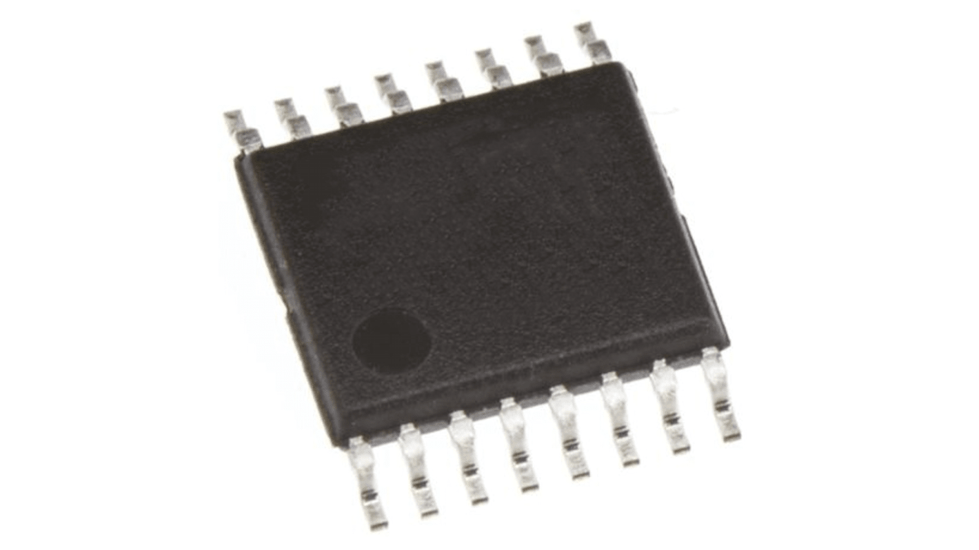
Renesas Electronics 5V2305PGGI Clock Buffer 16-Pin VFQFPN
- N° de stock RS:
- 254-4945
- Référence fabricant:
- 5V2305PGGI
- Fabricant:
- Renesas Electronics

Informations sur le stock actuellement non accessibles
- N° de stock RS:
- 254-4945
- Référence fabricant:
- 5V2305PGGI
- Fabricant:
- Renesas Electronics
Spécifications
Documentation technique
Législations et de normes
Détails du produit
Recherchez des produits similaires en sélectionnant un ou plusieurs attributs.
Sélectionner tout | Attribut | Valeur |
|---|---|---|
| Marque | Renesas Electronics | |
| Product Type | Clock Buffer | |
| Maximum Input Frequency | 200MHz | |
| Mount Type | Surface | |
| Maximum Propagation Delay Time | 3ns | |
| Package Type | VFQFPN | |
| Pin Count | 16 | |
| Minimum Supply Voltage | 2.3V | |
| Maximum Supply Voltage | 3.6V | |
| Minimum Operating Temperature | -40°C | |
| Maximum Operating Temperature | 85°C | |
| Series | IDT5V2305 | |
| Standards/Approvals | Pb-Free, RoHS | |
| Automotive Standard | No | |
| Sélectionner tout | ||
|---|---|---|
Marque Renesas Electronics | ||
Product Type Clock Buffer | ||
Maximum Input Frequency 200MHz | ||
Mount Type Surface | ||
Maximum Propagation Delay Time 3ns | ||
Package Type VFQFPN | ||
Pin Count 16 | ||
Minimum Supply Voltage 2.3V | ||
Maximum Supply Voltage 3.6V | ||
Minimum Operating Temperature -40°C | ||
Maximum Operating Temperature 85°C | ||
Series IDT5V2305 | ||
Standards/Approvals Pb-Free, RoHS | ||
Automotive Standard No | ||
The Renesas Electronics high performance, low skew clock buffer that operates up to 200 MHz. One bank of five outputs provides low skew copies of CLK. Through the use of control pin G, the outputs of bank Y(0:4) can be placed in a low state regardless of CLK input. The device operates in 2.5 V and 3.3 V environments. The built-in output enable glitch suppression ensures a synchronized output enable sequence to distribute full period clock signals. It is is characterized for operation from -40°C to +85°C.
High performance 1:5 clock driver for general purpose applications
Operates up to 170 MHz at VDD is 2.5 V
Operates up to 200 MHz at VDD is 3.3 V
Pin-to-pin skew < 75 ps at 3.3 V operation
VDD range is 2.3 V to 3.6 V
Output enable glitch suppression
Available in TSSOP and VFQFPN packages
Liens connexes
- Renesas Electronics Clock Buffer 16-Pin VFQFPN
- Renesas Electronics 5PB1214CMGK Clock Buffer 16-Pin VFQFPN
- Renesas Electronics 5PB1204CMGK Clock Buffer 16-Pin VFQFPN
- Renesas Electronics 9DMV0141AKILF Clock Buffer, 16-Pin 1 VFQFPN
- Renesas Electronics 5PB1106CMGI Clock Buffer, 16-Pin 4 VFQFPN
- Renesas Electronics 5PB1108CMGI Clock Buffer, 16-Pin 8 VFQFPN
- Renesas Electronics 5PB1108PGGI Clock Buffer, 16-Pin 8 VFQFPN
- Renesas Electronics 9DML4493ANLGI Clock Buffer 32-Pin VFQFPN