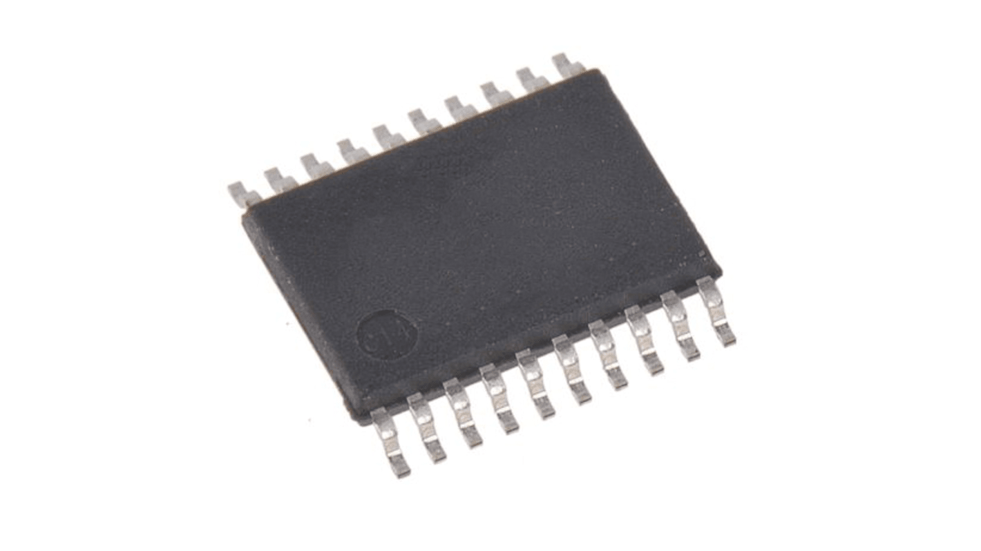
Renesas Electronics 5PB1110PGGI Clock Buffer 20-Pin TSSOP
- N° de stock RS:
- 254-4943P
- Référence fabricant:
- 5PB1110PGGI
- Fabricant:
- Renesas Electronics

Offre groupée disponible
Sous-total 10 unités (conditionné en tube)*
47,85 €
(TVA exclue)
57,90 €
(TVA incluse)
Informations sur le stock actuellement non accessibles - Veuillez vérifier plus tard
Unité | Prix par unité |
|---|---|
| 10 - 18 | 4,785 € |
| 20 - 24 | 4,685 € |
| 26 - 72 | 4,52 € |
| 74 + | 3,905 € |
*Prix donné à titre indicatif
- N° de stock RS:
- 254-4943P
- Référence fabricant:
- 5PB1110PGGI
- Fabricant:
- Renesas Electronics
Spécifications
Documentation technique
Législations et de normes
Détails du produit
Recherchez des produits similaires en sélectionnant un ou plusieurs attributs.
Sélectionner tout | Attribut | Valeur |
|---|---|---|
| Marque | Renesas Electronics | |
| Product Type | Clock Buffer | |
| Maximum Input Frequency | 200MHz | |
| Mount Type | Surface | |
| Maximum Propagation Delay Time | 2.5ns | |
| Package Type | TSSOP | |
| Pin Count | 20 | |
| Minimum Supply Voltage | 1.71V | |
| Maximum Supply Voltage | 3.47V | |
| Minimum Operating Temperature | -40°C | |
| Maximum Operating Temperature | 105°C | |
| Standards/Approvals | RoHS | |
| Height | 1.2mm | |
| Series | 5PB11xx | |
| Length | 6.6mm | |
| Width | 6.6 mm | |
| Automotive Standard | No | |
| Sélectionner tout | ||
|---|---|---|
Marque Renesas Electronics | ||
Product Type Clock Buffer | ||
Maximum Input Frequency 200MHz | ||
Mount Type Surface | ||
Maximum Propagation Delay Time 2.5ns | ||
Package Type TSSOP | ||
Pin Count 20 | ||
Minimum Supply Voltage 1.71V | ||
Maximum Supply Voltage 3.47V | ||
Minimum Operating Temperature -40°C | ||
Maximum Operating Temperature 105°C | ||
Standards/Approvals RoHS | ||
Height 1.2mm | ||
Series 5PB11xx | ||
Length 6.6mm | ||
Width 6.6 mm | ||
Automotive Standard No | ||
The Renesas Electronics high-performance LVCMOS clock buffer has an additive phase jitter of 50 fs RMS. There are five different fan-out variations available that is 1:2 to 1:10. Its supports a synchronous glitch-free output enable (OE) function to eliminate any potential intermediate incorrect output clock cycles when enabling or disabling outputs. It can operate from a 1.8 V to 3.3 V supply.
High-performance 1:2, 1:4, 1:6, 1:8, 1:10 LVCMOS clock buffer
Very low pin-to-pin skew: < 50 ps
Very low additive jitter: < 50 fs
Supply voltage: 1.8 V to 3.3 V
3.3 V tolerant input clock
fMAX is 200 MHz
Integrated serial termination for 50 Ω channel
Packaged in 8-, 14-, 16-, 20-pin TSSOP and as small as 2 x 2 mm DFN and 3 x 3 mm VFQFPN packages
Industrial (-40°C to +85°C) and extended (-40°C to +105°C) temperature ranges