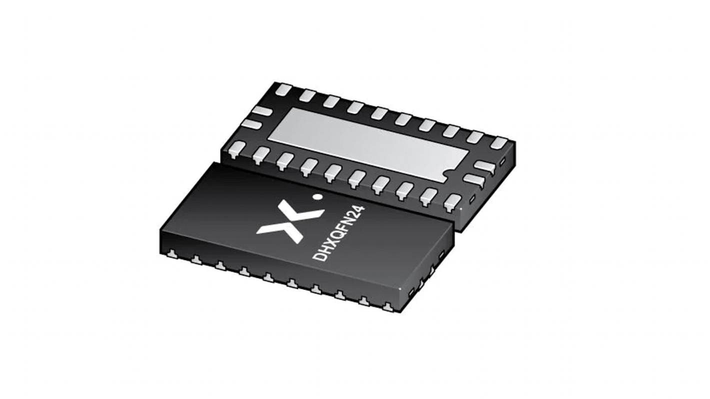
Nexperia Logic Level Translator, 8-Bit Non-Inverting TTL, 24-Pin SOT-8024
- N° de stock RS:
- 243-4423
- Référence fabricant:
- 74LVC8T245BZX
- Fabricant:
- Nexperia

Sous-total (1 bobine de 3000 unités)*
1 446,00 €
(TVA exclue)
1 749,00 €
(TVA incluse)
Frais de livraison offerts pour toute commande de plus de 75,00 €
Temporairement en rupture de stock
- Expédition à partir du 14 septembre 2026
Besoin de plus? Cliquez sur " Vérifier les dates de livraison " pour plus de détails
Unité | Prix par unité | la bobine* |
|---|---|---|
| 3000 + | 0,482 € | 1 446,00 € |
*Prix donné à titre indicatif
- N° de stock RS:
- 243-4423
- Référence fabricant:
- 74LVC8T245BZX
- Fabricant:
- Nexperia
Spécifications
Documentation technique
Législations et de normes
Détails du produit
Recherchez des produits similaires en sélectionnant un ou plusieurs attributs.
Sélectionner tout | Attribut | Valeur |
|---|---|---|
| Marque | Nexperia | |
| Logic Family | 74LVC | |
| Product Type | Logic Level Translator | |
| Logic Function | Translating Transceiver | |
| Number of Channels | 8 | |
| Polarity | Non-Inverting | |
| Mount Type | Surface | |
| Package Type | SOT-8024 | |
| Pin Count | 24 | |
| Minimum Supply Voltage | 3V | |
| Input Level | TTL | |
| Maximum Supply Voltage | 5.5V | |
| Minimum Operating Temperature | -40°C | |
| Maximum Propagation Delay Time @ CL | 4.1ns | |
| Output Level | TTL | |
| Maximum High Level Output Current | 24mA | |
| Maximum Operating Temperature | 125°C | |
| Series | 74LVC8T245 | |
| Standards/Approvals | RoHS | |
| Length | 2mm | |
| Height | 0.48mm | |
| Maximum Low Level Output Current | 24mA | |
| Width | 3.2 mm | |
| Output Type | 3 State | |
| Automotive Standard | No | |
| Sélectionner tout | ||
|---|---|---|
Marque Nexperia | ||
Logic Family 74LVC | ||
Product Type Logic Level Translator | ||
Logic Function Translating Transceiver | ||
Number of Channels 8 | ||
Polarity Non-Inverting | ||
Mount Type Surface | ||
Package Type SOT-8024 | ||
Pin Count 24 | ||
Minimum Supply Voltage 3V | ||
Input Level TTL | ||
Maximum Supply Voltage 5.5V | ||
Minimum Operating Temperature -40°C | ||
Maximum Propagation Delay Time @ CL 4.1ns | ||
Output Level TTL | ||
Maximum High Level Output Current 24mA | ||
Maximum Operating Temperature 125°C | ||
Series 74LVC8T245 | ||
Standards/Approvals RoHS | ||
Length 2mm | ||
Height 0.48mm | ||
Maximum Low Level Output Current 24mA | ||
Width 3.2 mm | ||
Output Type 3 State | ||
Automotive Standard No | ||
The Nexperia 8-bit dual supply translating transceivers with 3-state outputs that enable bidirectional level translation. They feature two data input-output ports (pins An and Bn), a direction control input (DIR), an output enable input (OE) and dual supply pins (VCC(A) and VCC(B)). Both VCC(A) and VCC(B) can be supplied at any voltage between 1.2 V and 5.5 V making the device suitable for translating between any of the low voltage nodes (1.2 V, 1.5 V, 1.8 V, 2.5 V, 3.3 V and 5.0 V). Pins An, OE and DIR are referenced to VCC(A) and pins Bn are referenced to VCC(B). A HIGH on DIR allows transmission from An to Bn and a LOW on DIR allows transmission from Bn to An.
Suspend mode
Latch-up performance exceeds 100 mA per JESD 78B Class II
±24 mA output drive (VCC = 3.0 V)
Inputs accept voltages up to 5.5 V
Low power consumption 30 μA maximum ICC
IOFF circuitry provides partial Power-down mode operation
Specified from -40 °C to +85 °C and -40 °C to +125 °C
The output enable input (OE) can be used to disable the outputs so the buses are effectively isolated. The devices are fully specified for partial power-down applications using IOFF. The IOFF circuitry disables the output, preventing any damaging backflow current through the device when it is powered down. In suspend mode when either VCC(A) or VCC(B) are at GND level, both A port and B port are in the high-impedance OFF-state. Active bus hold circuitry in the 74LVCH8T245 holds unused or floating data inputs at a valid logic level.
Liens connexes
- Nexperia 74LVC8T245BZX Logic Level Translator 24-Pin SOT-8024
- Nexperia 74AVC1T45GW Logic Level Translator Voltage Level Translator 6 Voltage Level Translator/Transceiver, 6-Pin
- Nexperia Level Translator 10 Voltage Level, 8-Pin VSSOP
- Nexperia 6-Pin SC-88
- Nexperia 74AVCH2T45DC Logic Level Translator Transceiver 8-Pin VSSOP
- onsemi TTL to CMOS, 16-Pin SOIC
- onsemi MC14504BDG TTL to CMOS, 16-Pin SOIC
- onsemi MC14504BDR2G TTL to CMOS, 16-Pin SOIC