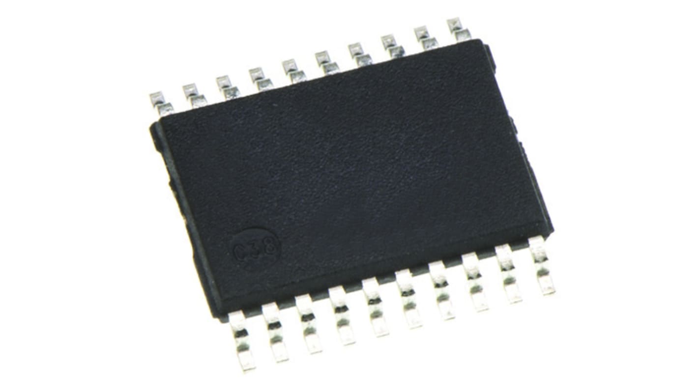
Toshiba 74VHCV541FT Schmitt Trigger Input 3 State Octal Bus Buffer, 20-Pin TSSOP
- N° de stock RS:
- 171-3407
- Référence fabricant:
- 74VHCV541FT
- Fabricant:
- Toshiba

Sous-total (1 paquet de 25 unités)*
7,35 €
(TVA exclue)
8,90 €
(TVA incluse)
Frais de livraison offerts pour toute commande de plus de 90,00 €
En stock
- 2 050 unité(s) prête(s) à être expédiée(s) d'un autre centre de distribution
Besoin de plus? Cliquez sur " Vérifier les dates de livraison " pour plus de détails
Unité | Prix par unité | le paquet* |
|---|---|---|
| 25 + | 0,294 € | 7,35 € |
*Prix donné à titre indicatif
- N° de stock RS:
- 171-3407
- Référence fabricant:
- 74VHCV541FT
- Fabricant:
- Toshiba
Spécifications
Documentation technique
Législations et de normes
Détails du produit
Recherchez des produits similaires en sélectionnant un ou plusieurs attributs.
Sélectionner tout | Attribut | Valeur |
|---|---|---|
| Marque | Toshiba | |
| Product Type | Octal Bus Buffer | |
| Logic Family | CMOS | |
| Logic Function | Buffer | |
| Schmitt Trigger Input | Yes | |
| Input Type | CMOS | |
| Mount Type | Surface | |
| Output Type | 3 State | |
| Package Type | TSSOP | |
| Minimum Supply Voltage | 1.8V | |
| Pin Count | 20 | |
| Maximum Supply Voltage | 5.5V | |
| Maximum Propagation Delay Time @ CL | 16.8ns | |
| Maximum High Level Output Current | -16mA | |
| Minimum Operating Temperature | -40°C | |
| Maximum Operating Temperature | 125°C | |
| Maximum Low Level Output Current | 16mA | |
| Length | 6.5mm | |
| Series | 74VHC | |
| Standards/Approvals | No | |
| Height | 1mm | |
| Supply Current | 2μA | |
| Automotive Standard | AEC-Q100 | |
| Sélectionner tout | ||
|---|---|---|
Marque Toshiba | ||
Product Type Octal Bus Buffer | ||
Logic Family CMOS | ||
Logic Function Buffer | ||
Schmitt Trigger Input Yes | ||
Input Type CMOS | ||
Mount Type Surface | ||
Output Type 3 State | ||
Package Type TSSOP | ||
Minimum Supply Voltage 1.8V | ||
Pin Count 20 | ||
Maximum Supply Voltage 5.5V | ||
Maximum Propagation Delay Time @ CL 16.8ns | ||
Maximum High Level Output Current -16mA | ||
Minimum Operating Temperature -40°C | ||
Maximum Operating Temperature 125°C | ||
Maximum Low Level Output Current 16mA | ||
Length 6.5mm | ||
Series 74VHC | ||
Standards/Approvals No | ||
Height 1mm | ||
Supply Current 2μA | ||
Automotive Standard AEC-Q100 | ||
The 74VHCV540FT and 74VHCV541FT are Advanced high speed CMOS OCTAL BUS BUFFERs fabricated with silicon gate CMOS technology. They achieve the high speed operation similar to equivalent Bipolar Schottky TTL while maintaining the CMOS low power dissipation. The 74VHCV540FT is an inverting type, and the 74VHCV541FT is a non-inverting type. When either G1 or G2 are high, the Terminal outputs are in the high-impedance state. Input pin have hysteresis between the positive-going and negative-going thresholds. Thus the 74VHCV540FT and 74VHCV541FT are capable of squaring up transitions of slowly changing input signals and provides an improved noise immunity. Input protection and output circuit ensure that 0 to 5.5 V can be applied to the input and output (Note) pins without regard to the supply voltage. These structure prevents device destruction due to mismatched supply and input/output voltages such as battery back up, hot board insertion, etc.
Wide operating temperature range: Topr = -40 to 125
High speed: tpd = 4.1 ns (typ.) at VCC = 5.0 V
Low power dissipation: ICC = 2.0 μA (max) at Ta = 25
Wide operating voltage range: VCC(opr) = 1.8 V to 5.5 V
Output current: |IOH|/IOL = 16 mA (min)(VCC = 4.5 V)
Power-down protection provided on all inputs and outputs.
Pin and function compatible with the 74 series (74AC/HC/AHC/LV etc.) 540 or 541 type
Liens connexes
- Toshiba Schmitt Trigger Input 3 State Octal Bus Buffer, 20-Pin TSSOP
- Toshiba 74HC126D Schmitt Trigger Input 3 State Octal Bus Buffer, 14-Pin SOIC
- Toshiba 3 State Octal Bus Buffer, 20-Pin TSSOP
- Toshiba 74VHCT125AFT Octal Bus Buffer, 14-Pin TSSOP
- Toshiba 74VHCT541AFT 3 State Octal Bus Buffer, 20-Pin TSSOP
- Toshiba 74VHC540FT 3 State Octal Bus Buffer, 20-Pin TSSOP
- Toshiba CMOS Octal Bus Buffer, 20-Pin TSSOP
- Toshiba 74LCX245FT CMOS Octal Bus Buffer, 20-Pin TSSOP