Infineon NOR 256Mbit SPI Flash Memory 24-Pin BGA, S25FL256SAGBHBA00

- N° de stock RS:
- 184-0052
- Référence fabricant:
- S25FL256SAGBHBA00
- Fabricant:
- Infineon
En cours d'approvisionnement - expédition le 01/05/2025, livraison sous 4 jour(s)
Ajouté
Prix L'unité (dans un plateau de 338)
5,411 €
(TVA exclue)
6,547 €
(TVA incluse)
| Unité | Prix par unité | le plateau* |
| 338 + | 5,411 € | 1 828,918 € |
| *prix conseillé | ||
- N° de stock RS:
- 184-0052
- Référence fabricant:
- S25FL256SAGBHBA00
- Fabricant:
- Infineon
Documentation technique
Législations et de normes
Détails du produit
This family of devices connect to a host system via a SPI. Traditional SPI single bit serial input and output (Single I/O or SIO) is
supported as well as optional two bit (Dual I/O or DIO) and four bit (Quad I/O or QIO) serial commands. This multiple width interface
is called SPI Multi-I/O or MIO. In addition, the FL-S family adds support for DDR read commands for SIO, DIO, and QIO that transfer
address and read data on both edges of the clock.
The Eclipse architecture features a Page Programming Buffer that allows up to 128 words (256 bytes) or 256 words (512 bytes) to be
programmed in one operation, resulting in faster effective programming and erase than prior generation SPI program or erase
algorithms.
Executing code directly from flash memory is often called Execute-In-Place or XIP. By using FL-S devices at the higher clock rates
supported, with QIO or DDR-QIO commands, the instruction read transfer rate can match or exceed traditional parallel interface,
asynchronous, NOR flash memories while reducing signal count dramatically.
The S25FL128S and S25FL256S products offer high densities coupled with the flexibility and fast performance required by a variety
of embedded applications. They are ideal for code shadowing, XIP, and data storage.
Spécifications
Attribut | Valeur |
|---|---|
| Memory Size | 256Mbit |
| Interface Type | SPI |
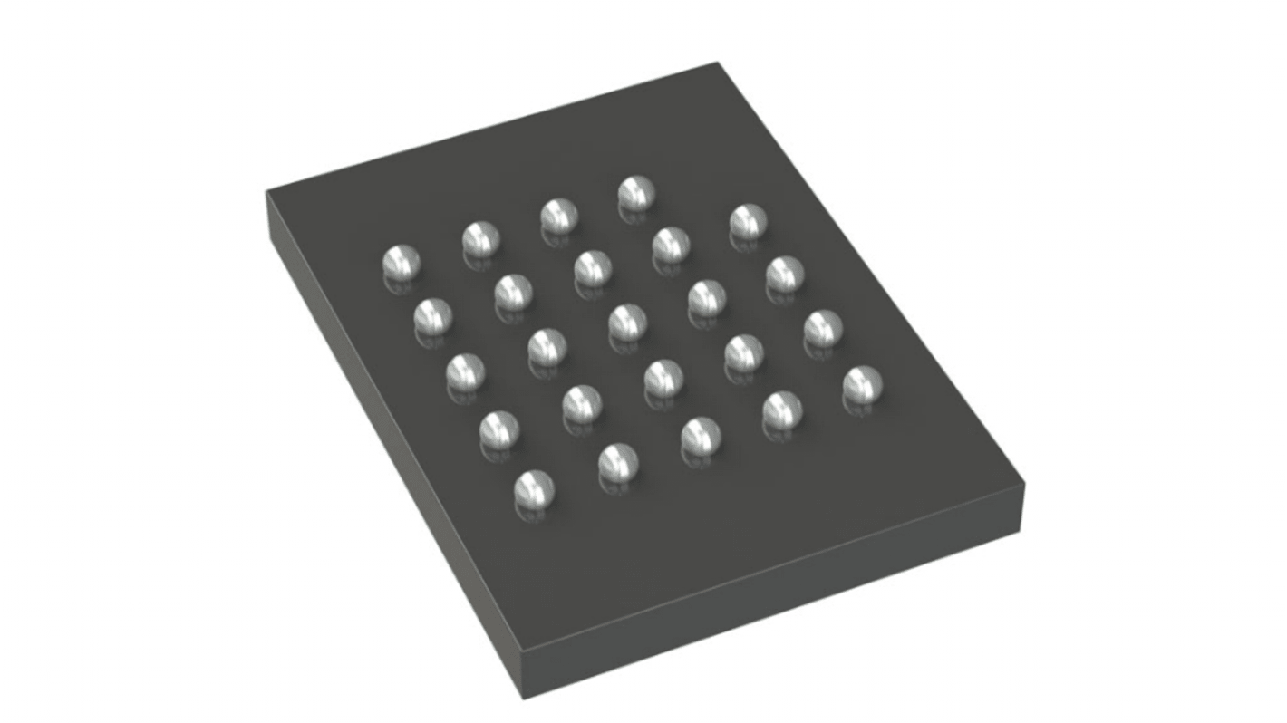
| Package Type | BGA |
| Pin Count | 24 |
| Organisation | 32M x 8 bit |
| Mounting Type | Surface Mount |
| Cell Type | NOR |
| Minimum Operating Supply Voltage | 2.7 V |
| Maximum Operating Supply Voltage | 3.6 V |
| Block Organisation | Symmetrical |
| Length | 10.3mm |
| Height | 2.55mm |
| Width | 7.5mm |
| Dimensions | 10.3 x 7.5 x 2.55mm |
| Maximum Operating Temperature | +85 °C |
| Automotive Standard | AEC-Q100 |
| Maximum Random Access Time | 14.5ns |
| Series | S25FL |
| Number of Words | 32M |
| Minimum Operating Temperature | -40 °C |
| Number of Bits per Word | 8bit |
- N° de stock RS:
- 184-0052
- Référence fabricant:
- S25FL256SAGBHBA00
- Fabricant:
- Infineon